Method for manufacturing soi substrate and soi substrate

a manufacturing method and technology for soi substrates, applied in semiconductor/solid-state device manufacturing, basic electric elements, electric apparatus, etc., can solve the problems of reducing the manufacturing yield of semiconductor elements and semiconductor devices, and achieve the effect of improving the manufacturing yield of semiconductor devices including the soi substrates and suppressing the generation of surface roughness

Inactive Publication Date: 2010-12-30
SEMICON ENERGY LAB CO LTD
View PDF14 Cites 24 Cited by
  • Summary
  • Abstract
  • Description
  • Claims
  • Application Information

AI Technical Summary

Benefits of technology

[0020]According to an embodiment of the disclosed invention, a region where gas is trapped is formed in part (the periphery) of the surface to be bonded. Accordingly, an SOI substrate having a semiconductor layer where generation of the surface roughness is suppressed can be provided. In addition, the manufacturing yield of a semiconductor device including the SOI substrate can be improved.

Problems solved by technology

Such a roughness on a surface causes various defects in a later step, which leads to reduction in the manufacturing yield of semiconductor elements and semiconductor devices as a result.

Method used


Image

  • Method for manufacturing soi substrate and soi substrate
  • Method for manufacturing soi substrate and soi substrate
  • Method for manufacturing soi substrate and soi substrate

Examples


embodiment 1

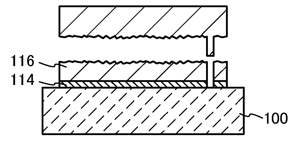
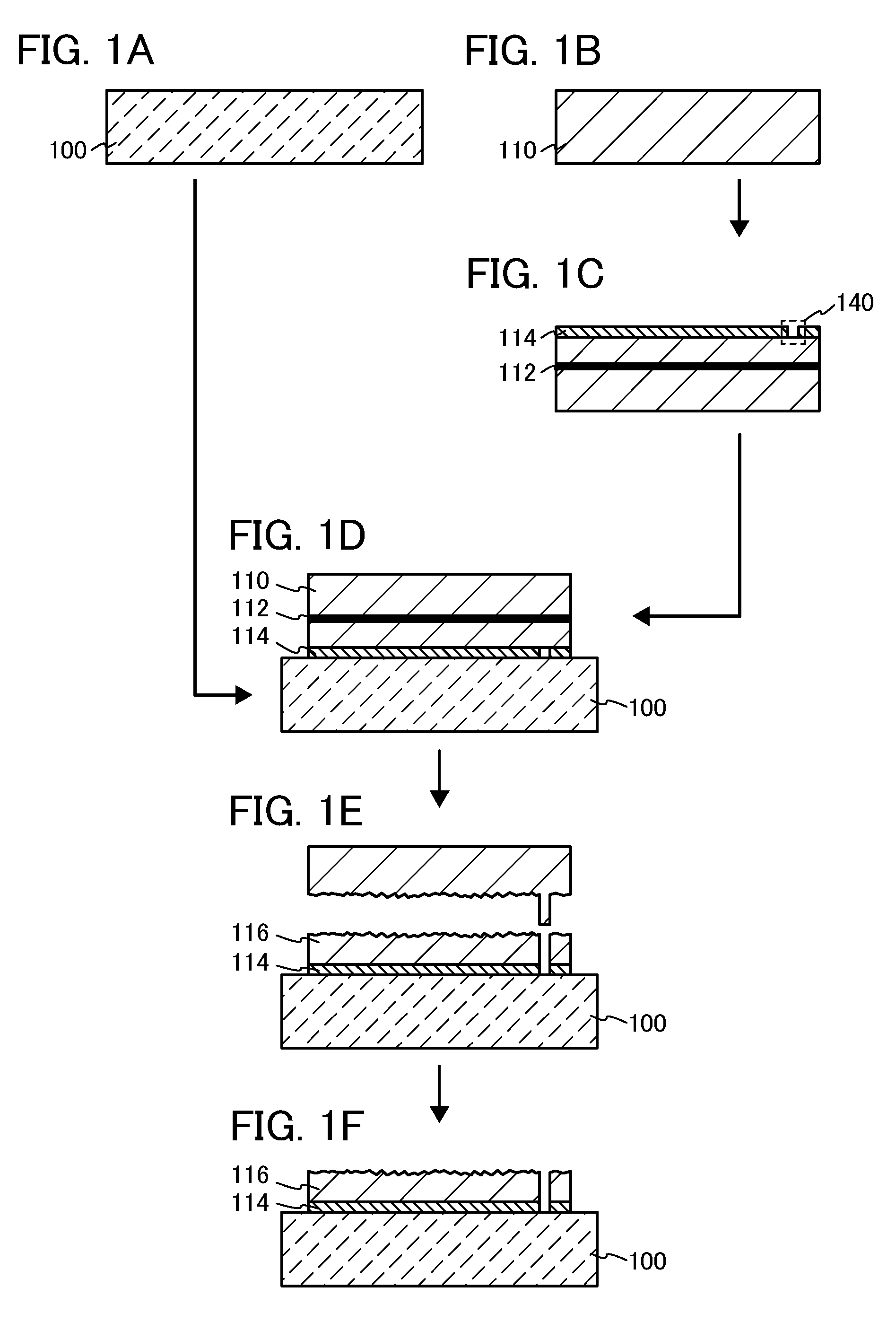
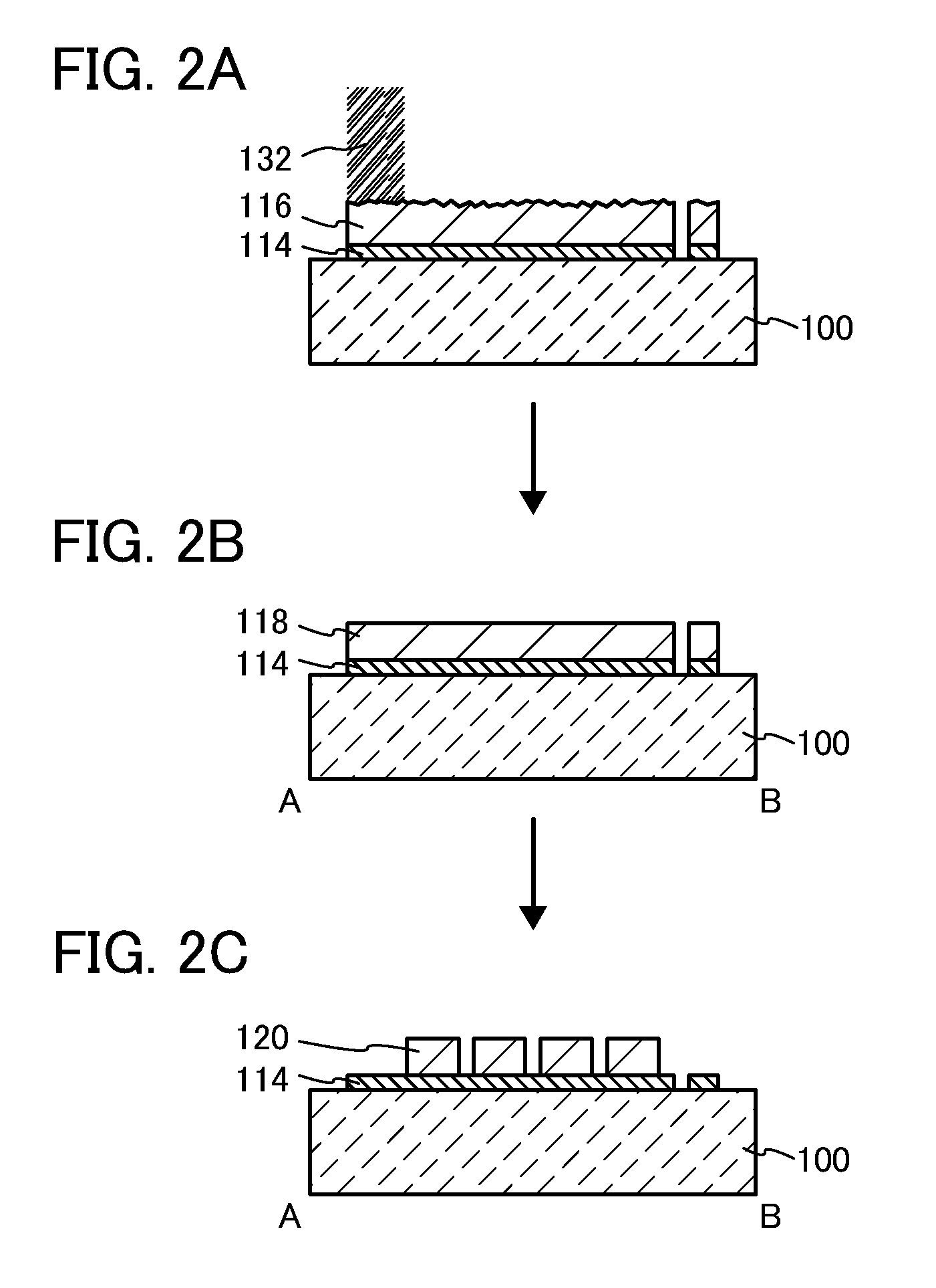
[0051]In this embodiment, an example of a method for manufacturing an SOI substrate is described with reference to drawings. Specifically, the case of manufacturing an SOI substrate where a single crystal semiconductor layer is provided over a base substrate is described.

[0052]First, a base substrate 100 and a bond substrate are prepared. Here, the case where a single crystal semiconductor substrate 110 is used as a bond substrate is described (see FIGS. 1A and 1B).

[0053]As the base substrate 100, a substrate formed using an insulator can be used. Specific examples thereof include: a variety of glass substrates used in the electronic industries, such as substrates formed using aluminosilicate glass, aluminoborosilicate glass, and barium borosilicate glass; a quartz substrate; a ceramic substrate; and a sapphire substrate. Note that when the glass substrate contains a larger amount of barium oxide (BaO) than boric acid (B2O3), more-practical heat-resistant glass can be obtained. Ther...

embodiment 2

[0106]In this embodiment, another example of a method for manufacturing an SOI substrate is described with reference to drawings.

[0107]First, the base substrate 100 and the single crystal semiconductor substrate 110 as a bond substrate are prepared (see FIG. 4A and FIG. 4C). The details of the base substrate 100 and the single crystal semiconductor substrate 110, for which Embodiment 1 can be referred to, are omitted here.

[0108]A recessed portion 142 is formed in the region at the surface of the base substrate 100, which corresponds to the periphery of the single crystal semiconductor substrate 110 (see FIG. 4B). Here, although the recessed portion 142 is formed at the surface of the base substrate 100, an embodiment of the disclosed invention is not limited to the formation of the recessed portion 142 as long as the closed region can be formed. Instead of the recessed portion, a projected portion or both the projected portion and the recessed portion may be formed. Embodiment 1 can...

embodiment 3

[0123]In this embodiment, another example of a method for manufacturing an SOI substrate is described with reference to drawings.

[0124]First, the base substrate 100 and the single crystal semiconductor substrate 110 as a bond substrate are prepared (see FIGS. 7A and 7C). The details of the base substrate 100 and the single crystal semiconductor substrate 110, for which Embodiment 1 or 2 can be referred to, are omitted here.

[0125]Next, a nitrogen-containing layer 102 (for example, a layer including an insulating film containing nitrogen, such as a silicon nitride (SiNx) film or a silicon nitride oxide (SiNxOy (x>y)) film) is formed over the surface of the base substrate 100 (see FIG. 7B).

[0126]The nitrogen-containing layer 102 formed in this embodiment functions as a layer (a bonding layer) to which the single crystal semiconductor layer is bonded in a later step. The nitrogen-containing layer 102 also functions as a barrier layer for preventing an impurity contained in the base subs...


PUM

PropertyMeasurementUnit
areaaaaaaaaaaa
temperatureaaaaaaaaaa
areaaaaaaaaaaa

Abstract

A bond substrate is irradiated with accelerated ions to form an embrittled region in the bond substrate; an insulating layer is formed over a surface of the bond substrate or a base substrate; the bond substrate and the base substrate are bonded to each other with the insulating layer interposed therebetween; a region in which the bond substrate and the base substrate are not bonded to each other and which is closed by the bond substrate and the base substrate is formed in parts of the bond substrate and the base substrate; the bond substrate is separated at the embrittled region by heat treatment; and a semiconductor layer is formed over the base substrate.

Description

BACKGROUND OF THE INVENTION[0001]1. Field of the Invention[0002]The present invention relates to a method for manufacturing a silicon-on-insulator (SOI) substrate, an SOI substrate, and a method for manufacturing a semiconductor device including the SOI substrate.[0003]2. Description of the Related Art[0004]In recent years, instead of a bulk silicon wafer, the use of a silicon-on-insulator (SOI) substrate where a thin single crystal semiconductor layer is provided over an insulating surface has been considered. Because parasitic capacitance generated by a drain of a transistor and a substrate can be reduced by use of an SOI substrate, SOI substrates have attracted great attention as substrates which improve performance of semiconductor integrated circuits.[0005]One of known methods for manufacturing SOI substrates is a Smart Cut (registered trademark) method (for example, see Patent Document 1). A summary of a method for manufacturing an SOI substrate by a Smart Cut method is descri...

Claims


Application Information

Patent Timeline
Patent Type & Authority Applications(United States)
IPC IPC(8): H01L21/762
CPCH01L21/02686H01L21/84H01L21/76254
Inventor OKUNO, NAOKISHIMOMURA, AKIHISATOKUNAGA, HAJIME
Owner SEMICON ENERGY LAB CO LTD
Why Eureka
Try Eureka