Light emitting module with optically-transparent thermally-conductive element

a technology of thermal conductors and light emitting modules, which is applied in the direction of solid-state devices, basic electric elements, electric devices, etc., can solve the problems of increasing the thermal load of the device, affecting the overall efficiency of the led, and adding cumbersome additional reflective surfaces to re-inject, etc., and achieves cost-effective effects. , the effect of prolonging the li

Active Publication Date: 2011-01-06
LUMILEDS HLDG BV
View PDF6 Cites 79 Cited by
  • Summary
  • Abstract
  • Description
  • Claims
  • Application Information

AI Technical Summary

Benefits of technology

[0031]According to a second aspect of the present invention, a method of manufacturing the light emitting module of the first aspect comprises the step of depositing the one or more inorganic layers of the OTTC element using one or more of the following evaporation or sputtering techniques: Plasma assisted or enhanced deposition, Ion Beam assisted deposition, electron beam assisted deposition, Remote Plasma assisted deposition, electron beam evaporation, open and closed field magnetron sputtering. The use of a low temperature deposition technique allows the unitary integrated module of the present invention to be fabricated with minimal introduction of thermally-induced stresses.
[0032]As will be appreciated by those skilled in the art, the present invention provides a compact and efficient light emitting module, which lends itself to mass production in cost effective fabrication process. The use of the inorganic OTTC element in the light emitting module allows for minimum colour temperature drift for the TEL and also further provides extended lifetime, even when used for high current drive applications.

Problems solved by technology

This leads to cumbersome additional reflective surfaces being introduced to re-direct and emit the wavelength converted light.
It is also not desirable to introduce reflective surfaces in the path of the emitted light as this may introduce optical loss affecting the overall efficiency of the LED.
Additionally, any optical loss will ultimately lead to increased phonon vibrations leading to increased thermal load in the device.
However, it does not result in a compact single integrated module, which can be fabricated in an efficient low cost in-line volume procedure.
However, infilling light transmissive material with thermally conductive materials causes modification in the optical transmissive properties of layer 108.
It is also noted that increased complexity in the preparation of the heat spreading plate is introduced, during preparation of the heat spreading plate material care has to be taken that the infilling material is uniformly dispersed in the resin otherwise adverse coagulation and flocculation of the thermal dissipating material arises increasing light loss in the material.

Method used


Image

  • Light emitting module with optically-transparent thermally-conductive element
  • Light emitting module with optically-transparent thermally-conductive element
  • Light emitting module with optically-transparent thermally-conductive element

Examples


Embodiment Construction

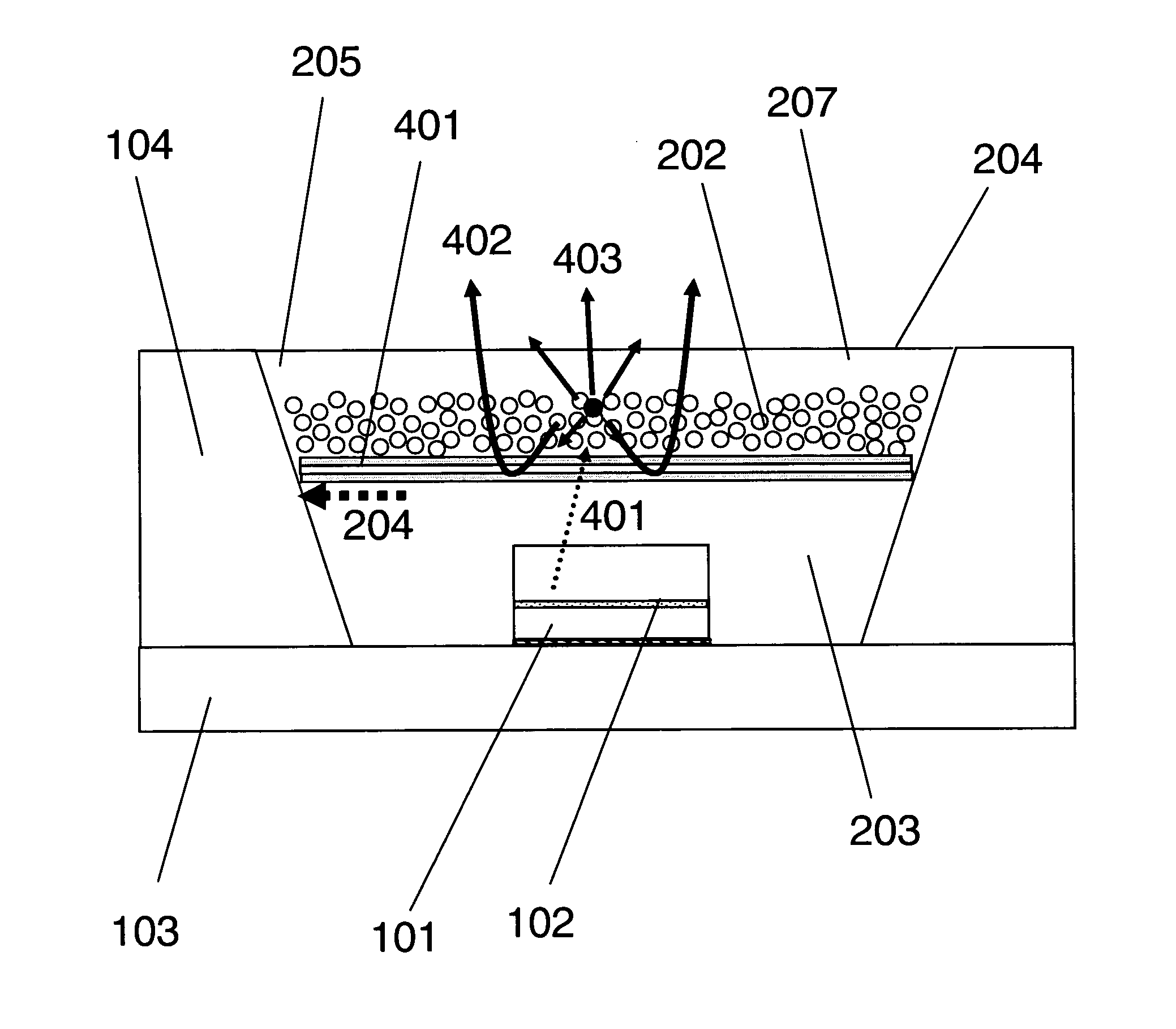
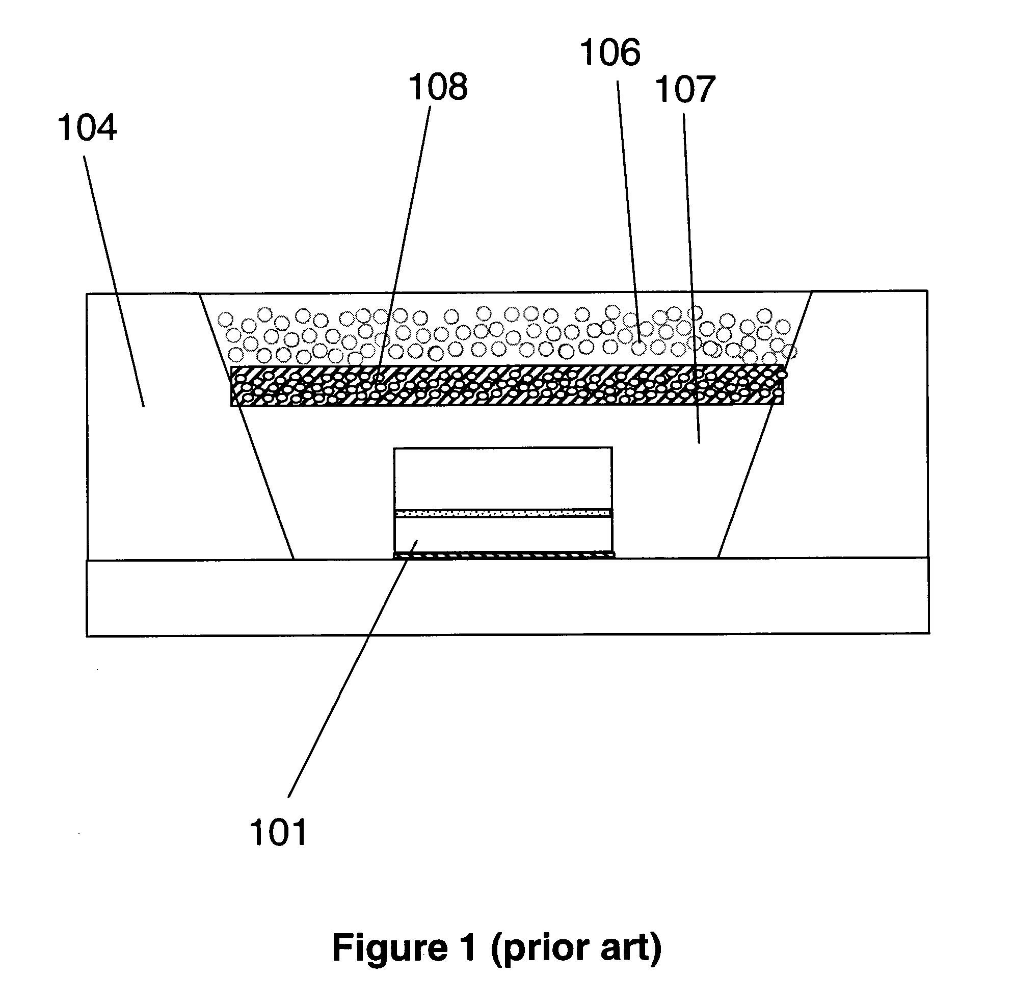
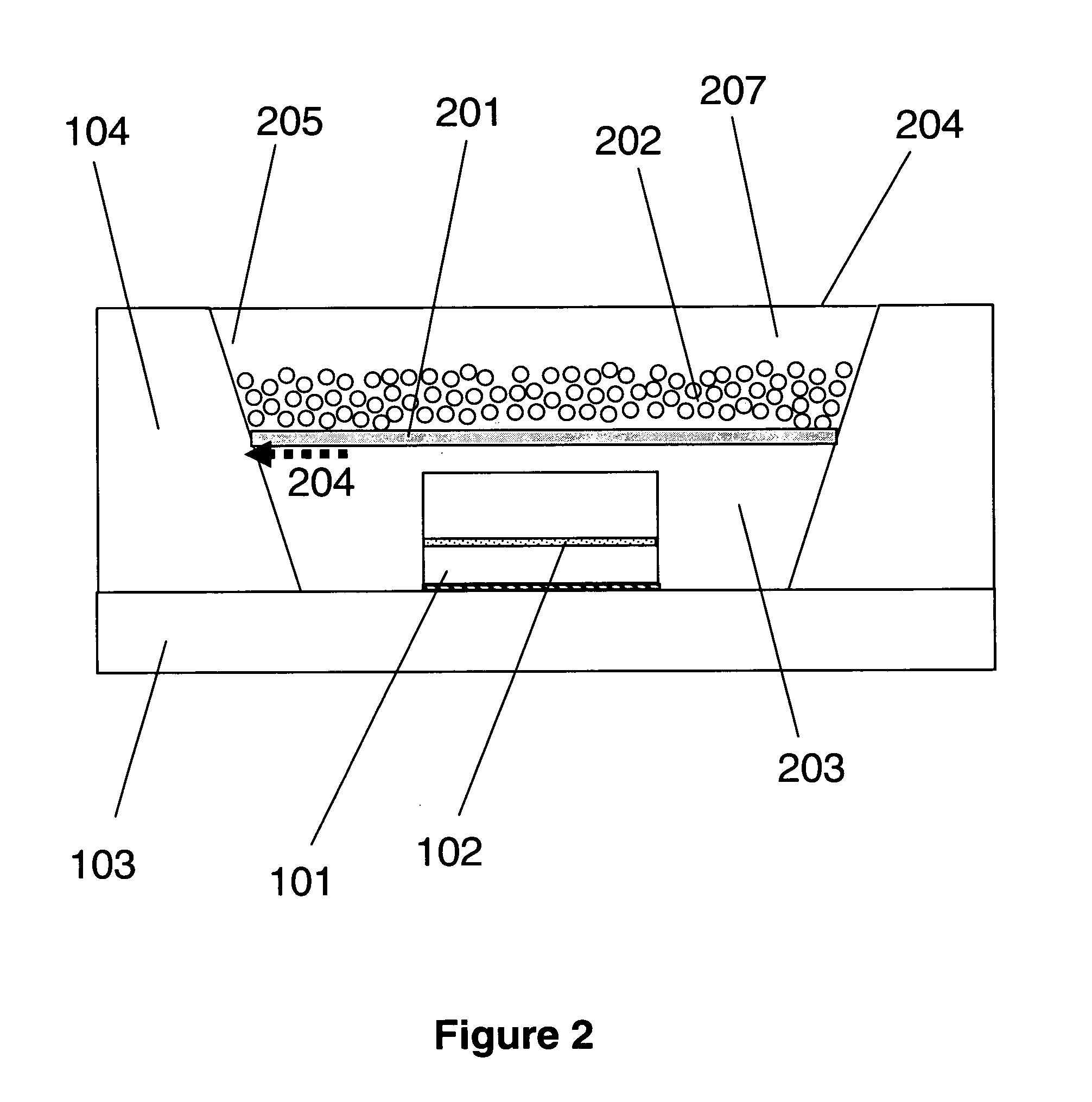
[0045]An object of the present invention is to provide a light emitting module comprising of a high luminous output semiconductor light emitting device and wavelength down converting material capable of withstanding a continuous high drive current and high power densities while still maintaining long lifetime and controlled colour temperatures with minimal degradation in characteristics of the wavelength converting element.

[0046]The invention can be incorporated in a light emitting device of any semiconductor material system such as, but not restricted to, InGaN, InGaP, InGaAs, InP, or ZnO. A GaN based light emitting diode (LED) having an epitaxial layer formed on a sapphire substrate is used as an example in the present invention. However, the present invention is not restricted to epitaxial layers grown on sapphire and may include Si, SiC, Ge, native free-standing GaN, AlN, LiAlO or any other growth and substrate technology. Additionally an LED with either a vertical or lateral cu...


PUM


Abstract

A light emitting module with improved optical functionality and reduced thermal resistance is described, which comprises a light emitting device (LED), a wavelength converting (WC) element and an inorganic optically-transmissive thermally-conductive (OTTC) element. The WC element is capable of absorbing light generated from the LED at a specific wavelength and re-emitting light having a different wavelength. The re-emitted light and any unabsorbed light exits through at least one surface of the module. The OTTC is in physical contact with the WC element and at least partially located in the optical path of the light. The OTTC comprises one or more layers of inorganic material having a thermal conductivity greater than that of the WC element. As such, a compact unitary integrated module is provided with excellent thermal characteristics, which may be further enhanced when the OTTC provides a thermal barrier for vertical heat propagation through the module but not lateral propagation.

Description

FIELD OF THE INVENTION[0001]The present invention relates to a solid state lighting module having a low thermal resistance and a method for producing such, which employs a wavelength converting element and an optically-transparent thermally-conducting element.BACKGROUND TO THE INVENTION[0002]Light emitting devices and diodes are based on a forward biased p-n junction. LEDs have recently reached high brightness levels that have allowed them to enter into new solid state lighting applications as well as replacements for high brightness light sources such as light engines for projectors and automotive car headlights. These markets have also been enabled by the economical gains achieved through the high efficiencies of LEDs, as well as reliability, long lifetime and environmental benefits. These gains have been partly achieved by use of LEDs that are capable of being driven at high currents and hence produce high luminous outputs while still maintaining high wall plug efficiencies.[0003...

Claims


Application Information

Patent Timeline
Patent Type & Authority Applications(United States)
IPC IPC(8): H01L33/50H01L33/44H01L33/58H01L33/64
CPCH01L33/507H01L33/58H01L33/644H01L2924/0002H01L2924/00H01L33/641
Inventor MCKENZIE, JAMES STUARTZOOROB, MAJD
Owner LUMILEDS HLDG BV
Why Eureka
Try Eureka