

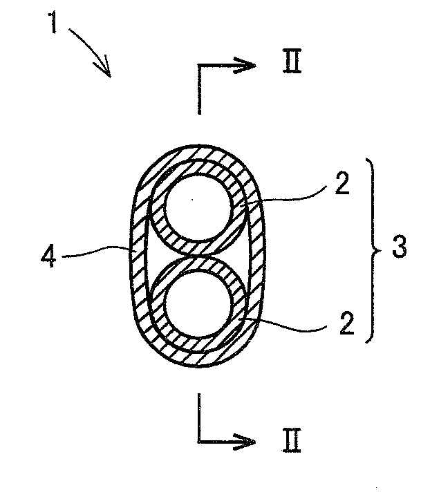
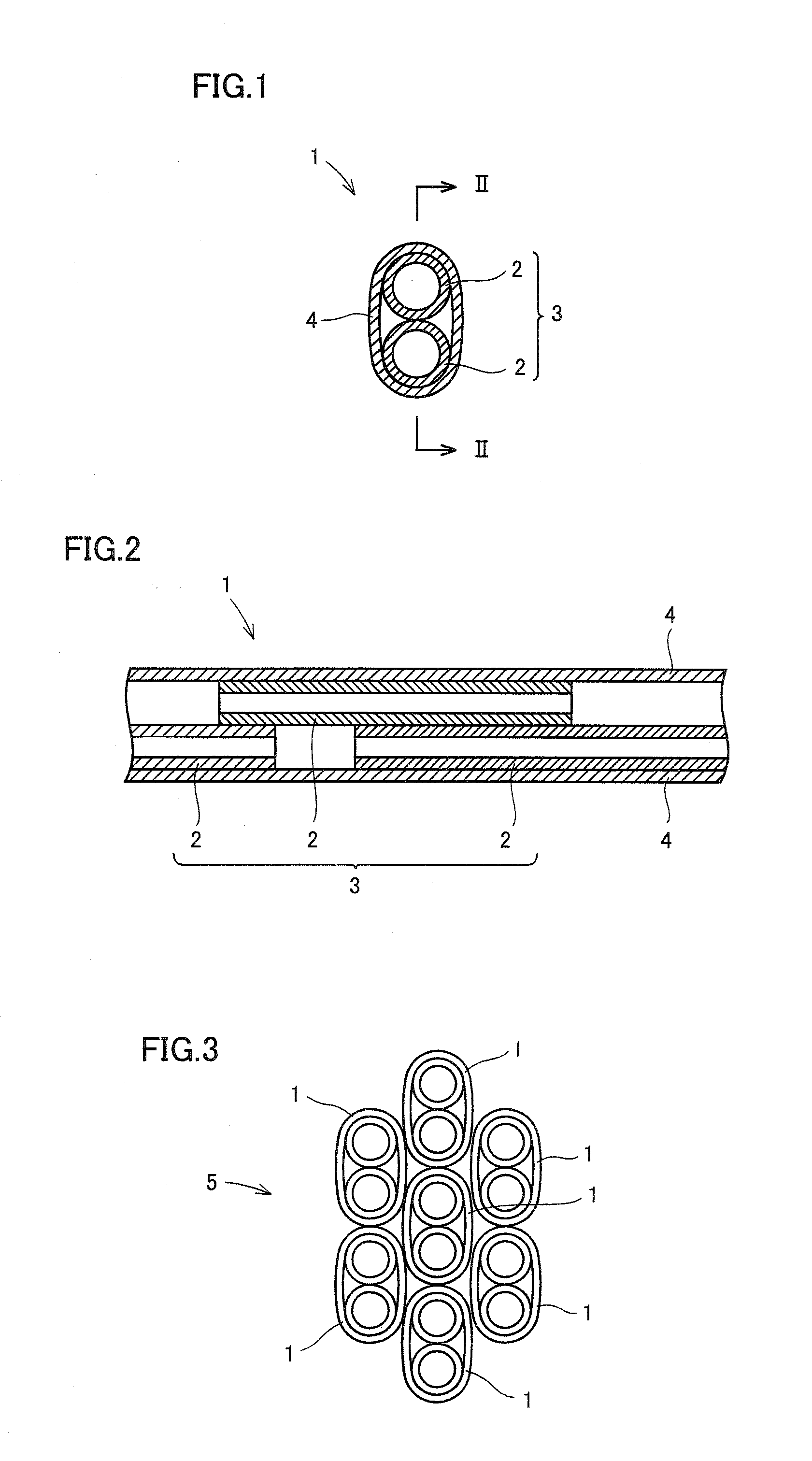
Carbon wire and NANO structure formed of carbon film and method of producing the same
a carbon film and nano-structure technology, applied in the direction of conductors, sustainable manufacturing/processing, final product manufacturing, etc., can solve the problems of high contact resistance, use these methods, and inability to provide a large area of graphite film essential to device application, etc., to achieve low resistance, low resistance carbon wire, and low resistance
- Summary
- Abstract
- Description
- Claims
- Application Information
AI Technical Summary
Benefits of technology
Problems solved by technology
Method used
Image

Examples
first embodiment
[0157]FIG. 10 is a schematic cross section of one example of a graphite film production apparatus used in the present invention.
[0158](Graphite Film Production Apparatus)
[0159]The present invention employs a graphite film production apparatus configured of quartz reaction tube 6 and alumina container 20 provided in quartz reaction tube 6 and having liquid Ga 1 introduced therein. Substrate 17 with amorphous carbon film 21 provided thereon is to be processed, placed in a vicinity of alumina container 20. External to quartz reaction tube 6, heater 7 is provided for the reaction tube to regulate the internal temperature of quartz reaction tube 6.
[0160]Substrate 17 may be a conventionally well known substrate that is used as a substrate for production of electrically conductive film. Preferably, an SiC, Ni, Fe, Mo, Pt or similar, monocrystalline substrate is used, as monocrystalline graphite film can be obtained.
[0161]Amorphous carbon film 21 may be provided in any conventional well kno...
second embodiment
[0167](Graphite Film Production Apparatus)
[0168]FIG. 11 is a schematic cross section of one example of a graphite film production apparatus used in the present invention when Ga vapor has uniform vapor pressure at a surface of a carbon source. A second embodiment employs a graphite film production apparatus having quartz reaction tube 6 and a subordinate Ga reaction chamber 22 provided in quartz reaction tube 6 and accommodating alumina container 20 having liquid Ga 9 introduced therein, and substrate 17 having amorphous carbon film 21 thereon, i.e., a substrate to be processed. Subordinate Ga reaction chamber 22 has a wall having a differential evacuation in the form of a small gap.
[0169]The first embodiment shows a graphite film production apparatus having quartz reaction tube 6 internally filled with Ga vapor 5 generated from liquid Ga 9. However, while a portion of quartz reaction tube 6 that is close to heater 7 is maintained at a predetermined high temperature, portions of qua...
third embodiment
[0175](Graphite Film Production Apparatus)
[0176]FIG. 12 is a schematic cross section of one example of a graphite film production apparatus employed in the present invention with Ga vapor plasmatized. A third embodiment employs a graphite film production apparatus having quartz reaction tube 6 accommodating alumina container 20 having liquid Ga 9 introduced therein, and a plasma producing electrode 10, with a heater 12 provided at the alumina container for Ga. Substrate 17 with amorphous carbon film 21 thereon, or a substrate to be processed, is positioned in a vicinity of alumina container 20 between paired plasma producing electrodes 10 and exposed to a Ga plasma 23. External to quartz reaction tube 6, heater 7 is provided for the reaction tube to regulate the internal temperature of quartz reaction tube 6.
[0177]Using Ga vapor to obtain graphite film is an effective technique to obtain a single or multiple layers of large-area graphite film and is a practical technique directed to...
PUM
| Property | Measurement | Unit |
|---|---|---|
| Temperature | aaaaa | aaaaa |
| Temperature | aaaaa | aaaaa |
| Temperature | aaaaa | aaaaa |
Abstract
Description
Claims
Application Information