Photosensitizer and solar cell using the same

Inactive Publication Date: 2011-01-20
SHARP KK
View PDF10 Cites 21 Cited by
  • Summary
  • Abstract
  • Description
  • Claims
  • Application Information

AI Technical Summary

Benefits of technology

[0021]The photosensitizer in accordance with the present invention includes an inorganic material carrying organic molecules that are molecules each having an aromatic ring. Since the organic molecules have aromatic rings, holes in the valence band of the inorganic material come to be more easily reduced. Thus, electrons and holes are reliably separated, and charge recombination can be prevented. As a result, life of the excited electrons in the inorganic material can be made longer, and electron injection to the inorganic material comes to be done with higher efficiency from the viewpoint of energy balance. Therefore, the photosensitizer including the inorganic material carrying such organic molecules has longer durability life and attains high incident photon-to-current conversion efficiency.

Problems solved by technology

Manufacturing cost of a crystalline silicon substrate or thin film silicon, however, is very high and hence, solar cells using these inevitably become very expensive.
At present, however, sufficiently high incident photon-to-current conversion efficiency has not been attained.

Method used


Image

  • Photosensitizer and solar cell using the same
  • Photosensitizer and solar cell using the same
  • Photosensitizer and solar cell using the same

Examples


example 1

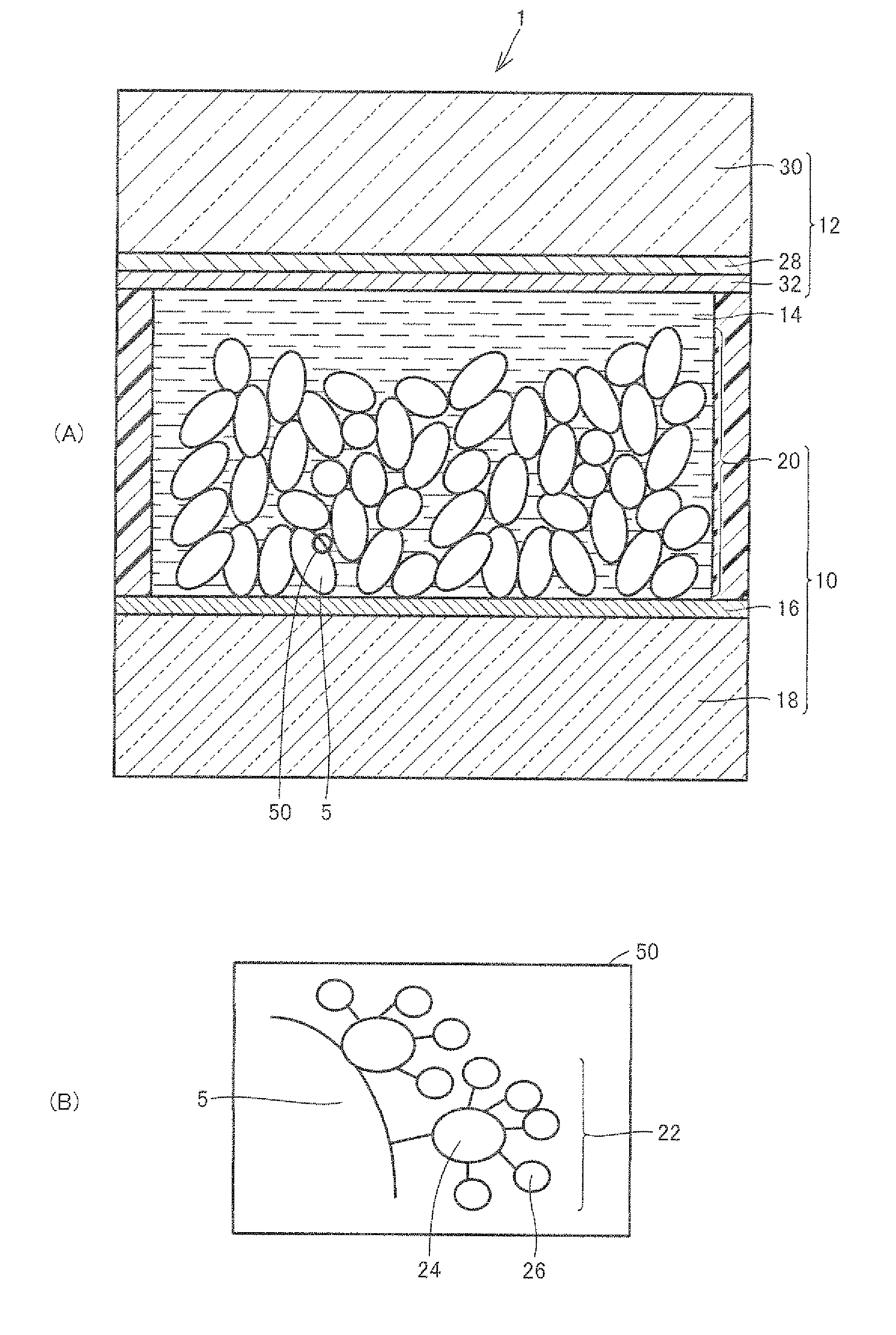
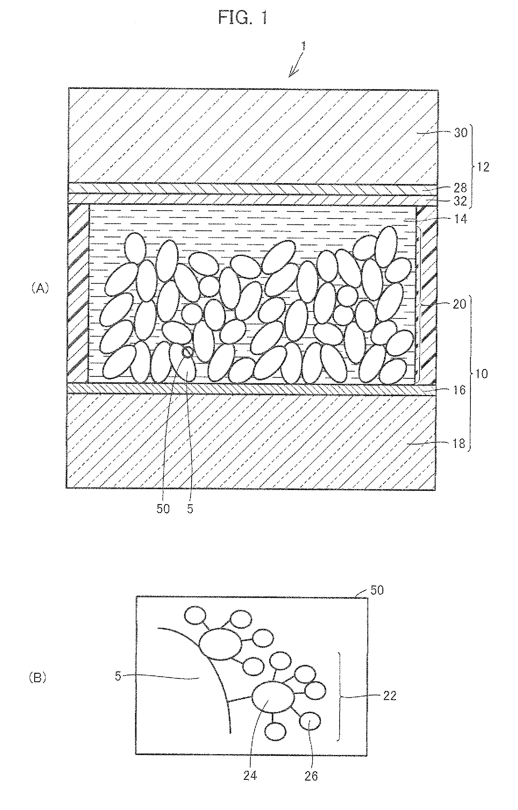
Manufacturing of Solar Cell

[0082](Fabrication of Semiconductor Electrode)

[0083]Commercially available titanium oxide paste (trade name: Ti-Nanoxide D / SP, manufactured by Soraronix, average particle size: 13 nm) was applied to a glass substrate (manufactured by Nippon Sheet Glass Co., Ltd.) as a substrate having a fluorine-doped tin oxide (FTO) film formed as a conductive film, by doctor blade method. Thereafter, the glass substrate was pre-dried for 30 minutes at 300° C., and thereafter sintered for 40 minutes at 500° C., and the pre-drying and sintering were repeated again. As a result, a porous semiconductor layer of titanium oxide film having the thickness of 12 μm was formed on the glass substrate.

[0084]According to the method described in Journal of the American Chemical Society (US), American Chemical Society, 1993, Vol. 115, pp. 8706-8715, quantum dots of cadmium sulfide (CdS) to be used as the inorganic material were manufactured. The quantum dots had the HOMO energy level o...

example 2

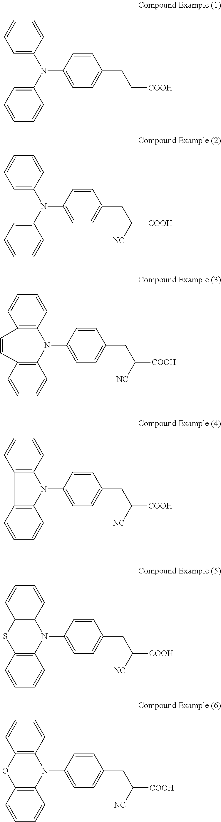
[0093]A solar cell of Example 2 was manufactured in the similar manner as Example 1 except that Compound Example (16) was used as the organic molecules.

example 3

[0094]A solar cell of Example 3 was manufactured in the similar manner as Example 1 except that Compound Example (17) was used as the organic molecules.


PUM


Abstract

A photosensitizer attaining high incident photon-to-current conversion efficiency and having long durability life and a solar cell using the photosensitizer are provided. A solar cell 1 includes: a semiconductor electrode 10 including a substrate 18 having a conductive film 16 formed on its surface and a porous semiconductor layer 20 formed on the substrate 18; a counter electrode 12 including a substrate 30 having a conductive film 28 formed on its surface; and a carrier transport layer 14 including conductive material, posed between the semiconductor electrode 10 and the counter electrode 12. The surface of porous semiconductor layer 20 is caused to carry a light absorber 22 including inorganic material 24 carrying organic molecules 26 each having an aromatic ring.

Description

TECHNICAL FIELD[0001]The present invention relates to a photosensitizer and a solar cell using the photosensitizer and, more specifically, to a photosensitizer with improved incident photon-to-current conversion efficiency and a solar cell using the same.BACKGROUND ART[0002]Recently, as an energy source alternative to fossil fuel, solar cells that can convert optical energy of sunlight to electric energy are attracting attention, and solar cells using crystalline silicon substrate or thin film silicon have come to be practically used. Manufacturing cost of a crystalline silicon substrate or thin film silicon, however, is very high and hence, solar cells using these inevitably become very expensive. In solar cells as such, in order to recover the cost on manufacturing, efforts have been made to reduce the cost per power output by improving the incident photon-to-current conversion efficiency. At present, however, sufficiently high incident photon-to-current conversion efficiency has ...

Claims


Application Information

Patent Timeline
IPC IPC(8): H01L51/44H01L51/46
CPCH01G9/2031H01G9/2054H01L2251/306Y02E60/12H01M14/005Y02E10/542H01M10/465H10K2102/102
Inventor HAN, LIYUANFUKE, NOBUHIROKOIDE, NAOKIISLAM, ASHRAFULFUKUI, ATSUSHI
Owner SHARP KK
Why Eureka
Try Eureka