Light emitting element

a technology of light-emitting elements and light-emitting devices, which is applied in the direction of discharge tubes/lamp details, discharge tubes/lamp details, luminescent compositions, etc., can solve the problems of low light-emitting efficiency and lower efficiency of light-emitting devices, and achieve high-efficiency light-emitting, facilitate light-emitting, and increase light-emitting efficiency

Active Publication Date: 2011-01-20
PANASONIC CORP
View PDF19 Cites 11 Cited by
  • Summary
  • Abstract
  • Description
  • Claims
  • Application Information

AI Technical Summary

Benefits of technology

[0017]In the light emitting device according to the present invention, each phosphor particle constituting the phosphor layer includes the n-type nitride semiconductor part and the p-type nitride semiconductor part. This facilitates light emission in each phosphor particle due to combination of electrons and holes, thereby increasing the light-emitting efficiency.
[0018]Further, in the light emitting device according to the present invention, at least one end surface, out of the end surfaces of each phosphor particle which are perpendicular to the c axis, is covered with the insulation film. When the c axe of the phosphor particle is perpendicular to the substrate, the insulation layer of the phosph...

Problems solved by technology

However, even when an electroluminescent device is fabricated using phosphor particles according to the conventional technique described in the Patent Document 1, there is the problem of a low light emitting efficiency.
The other one of them is that the conventional technique can not restrict the electric...

Method used


Image

  • Light emitting element
  • Light emitting element
  • Light emitting element

Examples


first embodiment

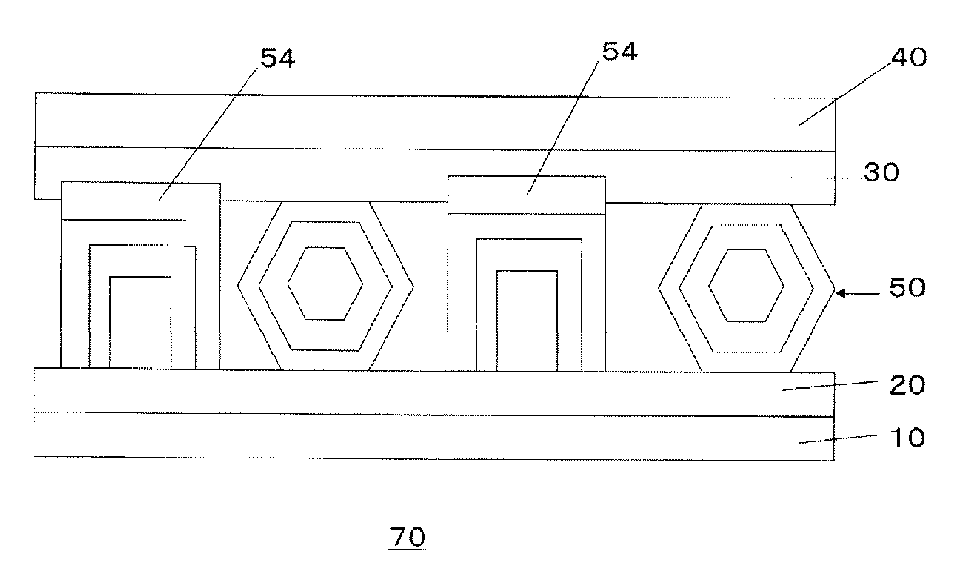
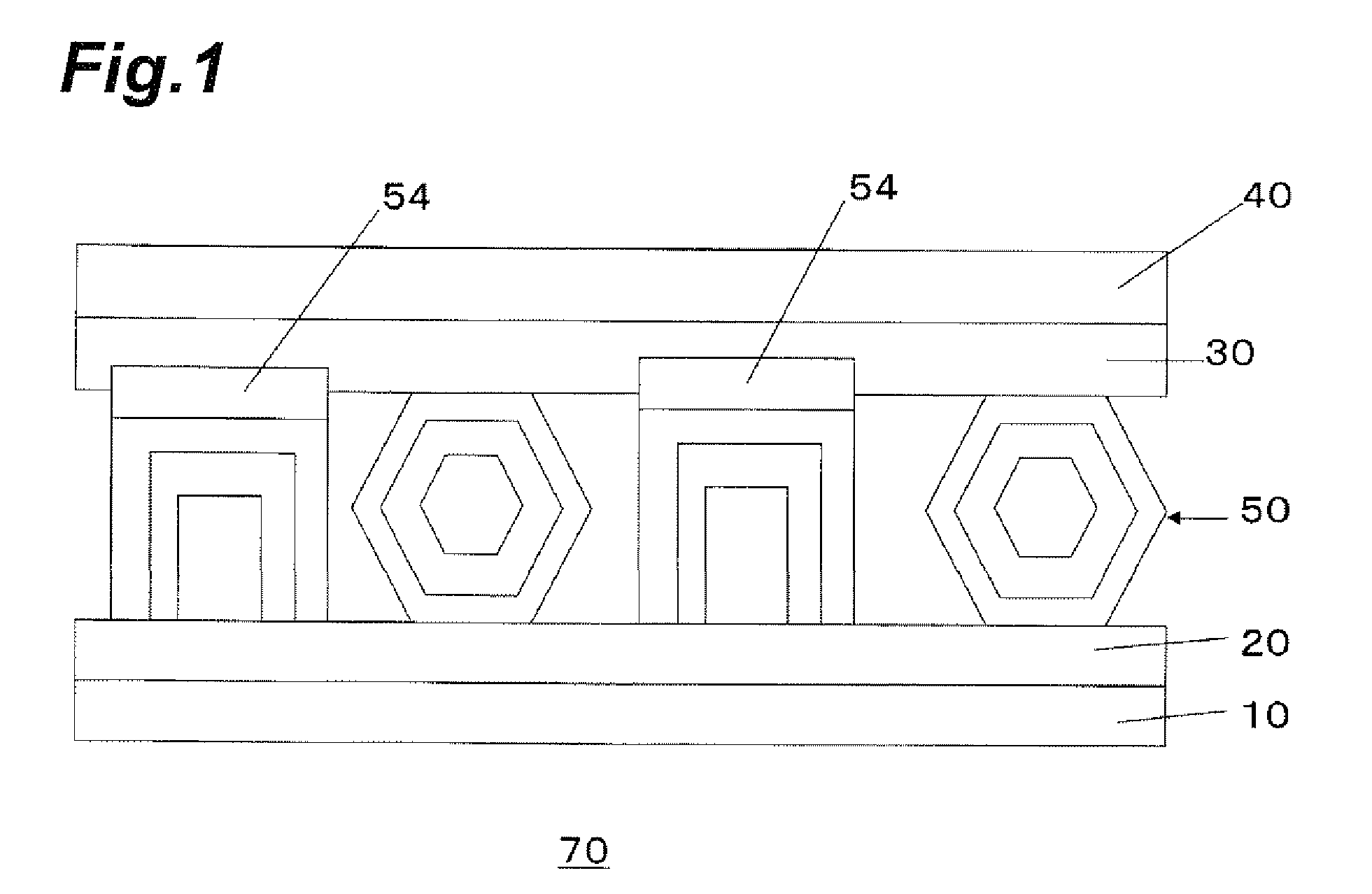
[0051]FIG. 1 is a cross-sectional view schematically illustrating the structure of a light emitting device 70 according to the present first embodiment. In the light emitting device 70, on a lower substrate 10, there are placed a lower electrode 20, phosphor particles 50, an upper electrode 30, and an upper substrate 40, in the mentioned order. In the light emitting device 70, the plurality of phosphor particles 50 placed between the lower electrode 20 and the upper electrode 30 form a phosphor layer. Further, FIG. 1 illustrates a minimum structure necessary for light emission, and other members may be provided in addition thereto.

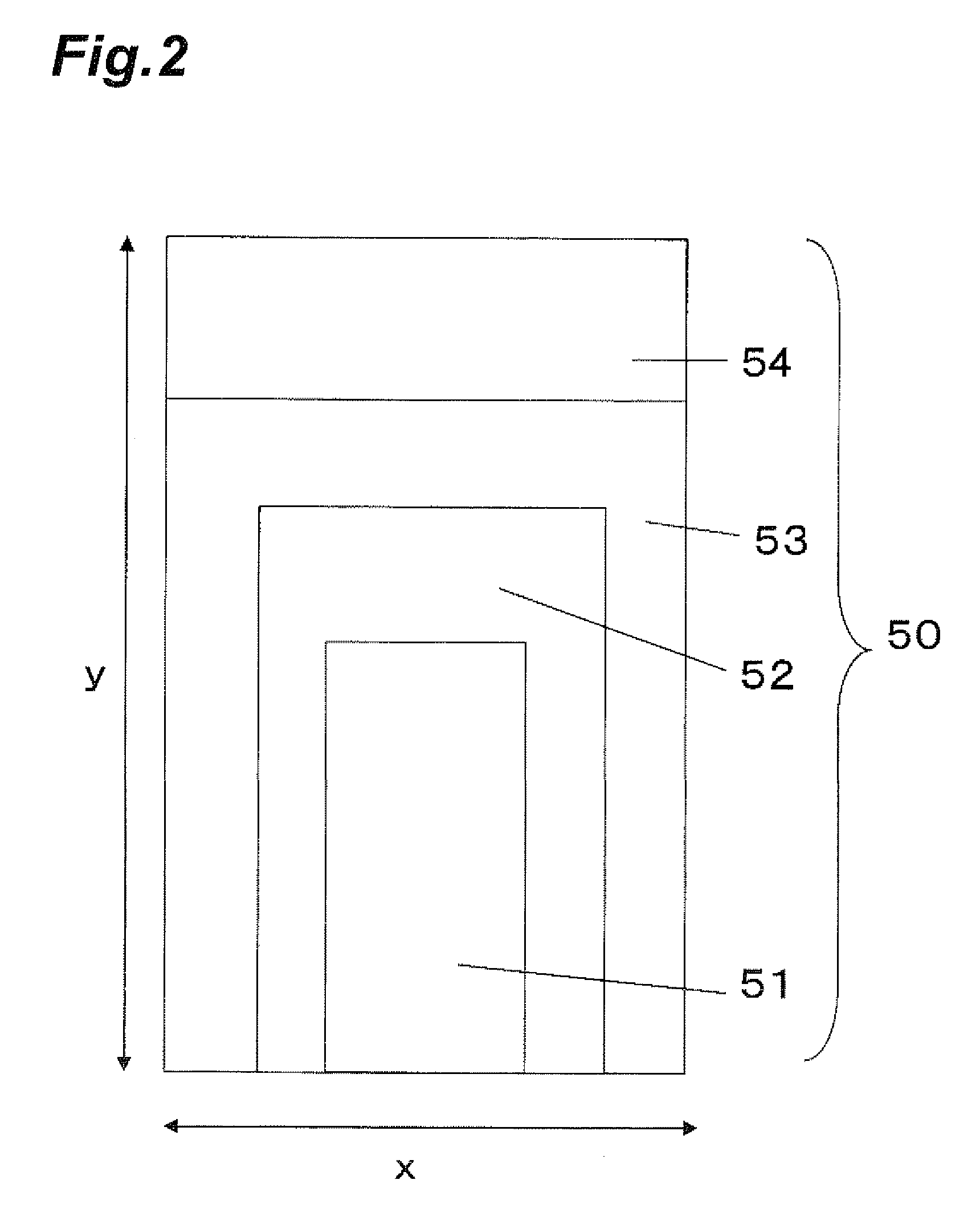
[0052]FIG. 2 is a cross-sectional view illustrating the cross-sectional structure of a phosphor particle 50 taken along the direction of the c axis thereof. FIG. 3 is a cross-sectional view illustrating the cross-sectional structure of the phosphor particle 50 taken along a plane perpendicular to the c axis thereof. In the light emitting device 70, each ph...

first example

[0076]Hereinafter, there will be described a method for fabricating a light emitting device according to the first example. In this case, at first, phosphor particles were formed, and the resultant phosphor particles were sandwiched between electrodes to form a light emitting device.

[0077](a) A sapphire substrate having a surface orientation of (0,0,0,1) and having a diameter of 5.08 cm (2 inches) was employed as a growth substrate 61. An SiO2 film with a thickness of 5 micrometers was formed as a growth mask 62 on the sapphire substrate 61 through a formation mask, through sputtering. It was formed through sputtering, using a SiO2 target as a target, in an atmosphere of an Ar gas. The growth mask 62 had hole portions with a diameter of 3 micrometers.

[0078](b) An AlN film was formed as nucleuses 51 thereon through sputtering. It was formed through sputtering, using an Al target as a target, in an atmosphere of an N2 gas. The AlN was grown in the direction of the c axis to have a thi...


PUM


Abstract

A light emitting device includes a pair of electrodes facing to each other and a phosphor layer which is sandwiched between the pair of electrodes and includes phosphor particles placed therein. The phosphor particles include an n-type nitride semiconductor part and a p-type nitride semiconductor part, the n-type nitride semiconductor part and the p-type nitride semiconductor part are made of respective single crystals having wurtzite-type crystal structures having c axes parallel with each other, and the phosphor particles include an insulation layer provided to overlie one end surface out of their end surfaces perpendicular to the c axes.

Description

BACKGROUND[0001]1. Technical Field[0002]The present invention relates to a light emitting element / device which is operated by a direct voltage applied thereto.[0003]2. Background Art[0004]Attention has been focused on nitride semiconductors, as practical semiconductor materials for use in light emitting devices, particularly blue-LEDs; blue light emitting diodes and UV-LEDs; Ultra-violet light emitting diodes, among light emitting devices which are operated by application of direct currents thereto. Particularly, attention has been focused on GaN based semiconductors which are represented by gallium nitride (GaN), indium gallium nitride (InGaN) mixed crystals, aluminum gallium nitride (AlGaN) mixed crystals, indium aluminum gallium nitride (InAlGaN) mixed crystals. Researches and developments have been actively conducted regarding these GaN-based semiconductors.[0005]Conventionally, such GaN-based semiconductors have been fabricated as single-crystal thin films by growing the semico...

Claims


Application Information

Patent Timeline
IPC IPC(8): H01L33/32H01L33/24
CPCC09K11/025H01L33/24H01L33/08C09K11/642
Inventor SHIMAMURA, TAKAYUKIONO, MASAYUKITANIGUCHI, REIKOSATOH, EIICHIMURAYAMA, MASATOODAGIRI, MASARU
Owner PANASONIC CORP
Why Eureka
Try Eureka