Semiconductor device and method for manufacturing same

a semiconductor and semiconductor technology, applied in the direction of semiconductor devices, electrical devices, transistors, etc., can solve the problems of difficult control of threshold voltage, difficult operation of p-channels, and difficulty in achieving heterojunction as intended, so as to achieve enhanced mode and increase the effect of turn-on voltag

Active Publication Date: 2011-02-03
SONY CORP
View PDF5 Cites 31 Cited by
  • Summary
  • Abstract
  • Description
  • Claims
  • Application Information

AI Technical Summary

Benefits of technology

[0021]In the semiconductor device according to the embodiment of the present invention, an n-channel high electron mobility transistor and a p-channel field-effect transistor are formed on the same compound semiconductor substrate. The n-channel field-effect transistor includes a first channel layer; an n-type first barrier layer that forms a heterojunction with the first channel layer, and supplies an n-type charge to the first channel layer; and a p-type gate region that has a pn junction-type potential barrier against the n-type first barrier layer. The p-channel field-effect transistor includes a p-type second channel layer, and an n-type gate region that has a pn junction-type potential barrier against the p-type second channel layer. Because the gate region of each transistor has a pn junction-type potential barrier, the turn-on voltage can be increased more than that in the Schottky barrier. Further, the control of threshold voltage and the operation in an enhancement mode can be realized with ease while reducing the reversed gate leak current.

Problems solved by technology

However, because the heterojunction is formed using an epitaxial growth method performed at a temperature of about 600° C., the annealing temperature of 800° C. or more causes the interdiffusion of the compound composition element or impurity element to occur at the heterojunction interface, making it difficult to realize the heterojunction as intended.
It is therefore difficult to control the threshold voltage, or to operate the p-channel field-effect transistor in an enhancement mode.
This presents a problem in realizing complementary transistors with reduced leak current by forming an n-channel field-effect transistor and a p-channel field-effect transistor on the same substrate.

Method used


Image

  • Semiconductor device and method for manufacturing same
  • Semiconductor device and method for manufacturing same
  • Semiconductor device and method for manufacturing same

Examples


first embodiment

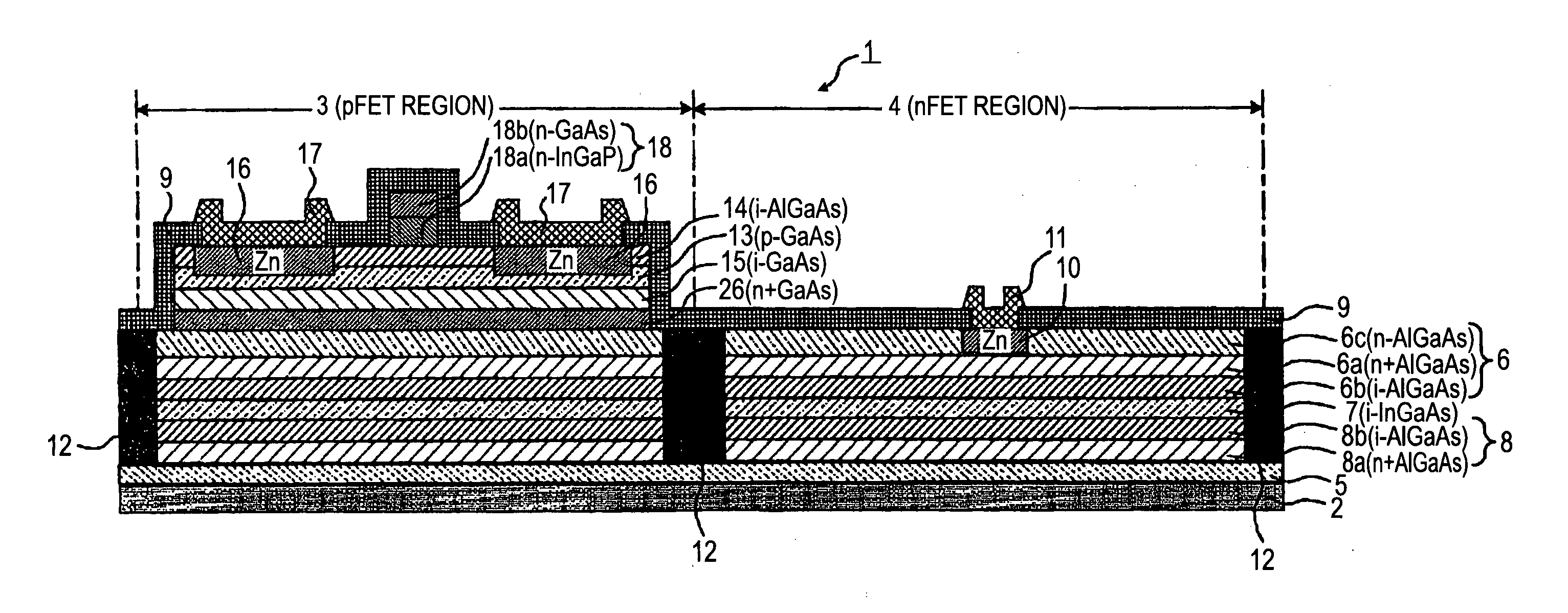
[0048]FIG. 1 is a schematic longitudinal sectional view of a semiconductor device according to First Embodiment of the present invention. The following detailed description will be given through the case where group III-V compounds are used for the compound semiconductor. First, an nFET region 4 is described. A GaAs monocrystalline substrate is used as a compound semiconductor substrate 2. A first buffer layer 5 is a non-doped i-GaAs layer with no impurities. An n-type second barrier layer 8 has a bilayer structure including an n-type charge supply layer 8a and a high-resistance layer 8b. The n-type charge supply layer 8a is an n+AlGaAs layer doped with the n-type impurity Si a high concentration of 1.0×10¹² to 4.0×10¹² atoms / cm2, and that has a thickness of about 3 nm. The high-resistance layer 8b is an i-AlGaAs layer with no impurities and having a thickness of about 3 nm. The first channel layer 7 is an i-InGaAs layer with no impurities and having a thickness of 5 nm to 15 nm. Th...

second embodiment

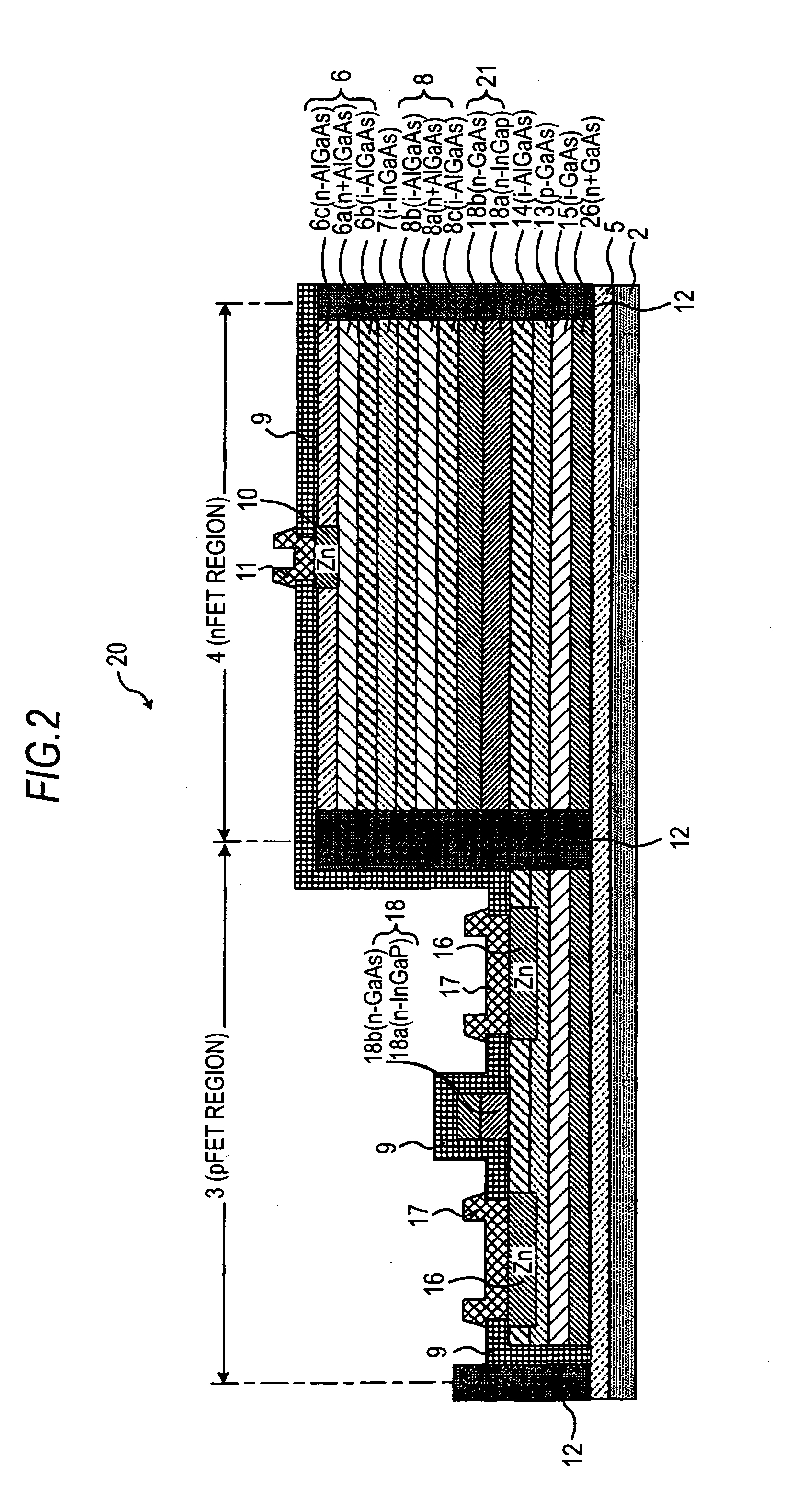
[0056]FIG. 2 is a schematic longitudinal sectional view of a semiconductor device 20 according to Second Embodiment of the present invention. Like numerals represent like members or members with similar functions.

[0057]The semiconductor device 20 includes a pFET region 3 and an nFET region 4 formed on a compound semiconductor substrate 2. The pFET region 3 is described first. A first buffer layer 5 of GaAs with no impurities is formed on the compound semiconductor substrate 2 of GaAs monocrystals. A cap layer 26 of n+GaAs doped with n-type impurities, and a second buffer layer 15 of i-GaAs with no impurities are formed on the first buffer layer 5. A second channel layer 13 of p−GaAs doped with p-type impurities is formed thereon.

[0058]A gate-leak prevention layer 14 of i-AlGaAs with no impurities is formed on the second channel layer 13. On the gate-leak prevention layer 14 is formed an n-type gate region 18 of a bilayer structure that includes an n-type first gate layer 18a of n−In...

third embodiment

[0064]A manufacturing method of a semiconductor device 1 according to Third Embodiment of the present invention is described below with reference to FIG. 3 to FIG. 11. Like numerals represent like members or members with similar functions.

[0065]FIG. 3 is a schematic longitudinal sectional view representing a laminate structure formed by the epitaxial growth of layers of primarily GaAs material on a GaAs monocrystalline substrate using, for example, a MOCVD (Metal. Organic Chemical Vapor Deposition) method. A GaAs layer with no impurities is epitaxially grown on a compound semiconductor substrate 2 of GaAs monocrystals to form a first buffer layer 5 of about 200 nm thick. Then, an n+AlGaAs layer doped with the n-type impurity Si at a high concentration of 1.0×10¹² to 4.0×10¹² atoms / cm2, for example, 3.0×10¹² atoms / cm2 is epitaxially grown on the first buffer layer 5 to form an n-type charge supply layer 8a of about 3 nm thick. This is followed by the epitaxial growth of a i-AlGaAs la...


PUM


Abstract

A semiconductor device includes: a compound semiconductor substrate; an n-channel field-effect transistor region formed on the compound semiconductor substrate, and that includes a first channel layer; an n-type first barrier layer that forms a heterojunction with the first channel layer, and supplies an n-type charge to the first channel layer; and a p-type gate region that has a pn junction-type potential barrier against the n-type first barrier layer; and a p-channel field-effect transistor region formed on the compound semiconductor substrate, and that includes a p-type second channel layer, and an n-type gate region that has a pn junction-type potential barrier against the p-type second channel layer.

Description

BACKGROUND OF THE INVENTION[0001]1. Field of the Invention[0002]The present invention relates to compound semiconductor field-effect transistors, particularly to semiconductor devices that include an n-type high electron mobility transistor and p-type field-effect transistor formed on the same compound semiconductor substrate. 2. Description of the Related Art[0003]Field-effect transistors with a compound semiconductor layer of a material such as GaAs have high electron mobility and desirable frequency characteristics, and for this reason have been widely used with an n-channel for high-frequency region applications such as in cellular phones. The n-channel FET (Field Effect Transistor) currently in use for the high frequency band is the high electron mobility transistor (HEMT). Its variant pseudomorphic high electron mobility transistor (PHEMT; Pseudomorphic HEMT) is also known that tolerates certain degrees of lattice mismatch in epitaxial growth, and thus realizes even higher ele...

Claims


Application Information

Patent Timeline
Patent Type & Authority Applications(United States)
IPC IPC(8): H01L27/085H01L21/8238H01L21/335H01L29/778
CPCH01L21/8252H01L27/0605H01L29/7787H01L29/205H01L29/66462H01L27/098H01L2924/13064
Inventor TAMARI, SHINICHINAKAMURA, MITSUHIROWAKIZONO, KOJINISHIDA, TOMOYAIBUSUKI, YUJI
Owner SONY CORP
Why Eureka
Try Eureka