Method of Passivating and Reducing Reflectance of a Photovoltaic Cell

a photovoltaic cell and passivating technology, applied in the direction of semiconductor/solid-state device manufacturing, electrical apparatus, semiconductor devices, etc., can solve the problems of high cost of implementation of vacuum deposition techniques, thin silicon nitride layer also reduces the reflectance of the pv cell, and achieves excellent passivation properties of silicon nitride, reduce the cost of manufacturing silicon pv cells, and reduce the effect of the cos

Inactive Publication Date: 2011-02-10
ENERGY FOCUS INC
View PDF23 Cites 21 Cited by
  • Summary
  • Abstract
  • Description
  • Claims
  • Application Information

AI Technical Summary

Benefits of technology

[0008]The foregoing method utilizes the excellent passivation properties of silicon nitride while also reducing the reflectance of a silicon PV cell.
[0009]Preferred embodiments of the invention utilize a liquid phase deposition process using material produced through Sol-Gel chemical methods to provide an index-matching film structure atop the silicon nitride passivation layer. This results in a significantly lowered cost for manufacturing silicon PV cells because liquid phase deposition techniques are overall less expensive to implement and can be accomplished through a variety of means.

Problems solved by technology

The relatively thick silicon nitride layer also reduces the reflectance of the PV cell, due to its relatively high index of refraction.
One drawback of using silicon nitride for the dual purposes of passivating and reducing reflectance of a PV cell is that the silicon nitride layer is typically formed using a vacuum deposition process.
Vacuum deposition techniques are costly to implement and require the largest and most expensive equipment used in PV cell fabrication.
Not surprisingly, extensive use of vacuum deposition machines increases the total cost of manufacturing PV cells.
A further drawback of using silicon nitride for reducing reflectance of a PV cell is that its ability to reduce reflectance is limited in comparison to other materials.

Method used


Image

  • Method of Passivating and Reducing Reflectance of a Photovoltaic Cell
  • Method of Passivating and Reducing Reflectance of a Photovoltaic Cell
  • Method of Passivating and Reducing Reflectance of a Photovoltaic Cell

Examples


Embodiment Construction

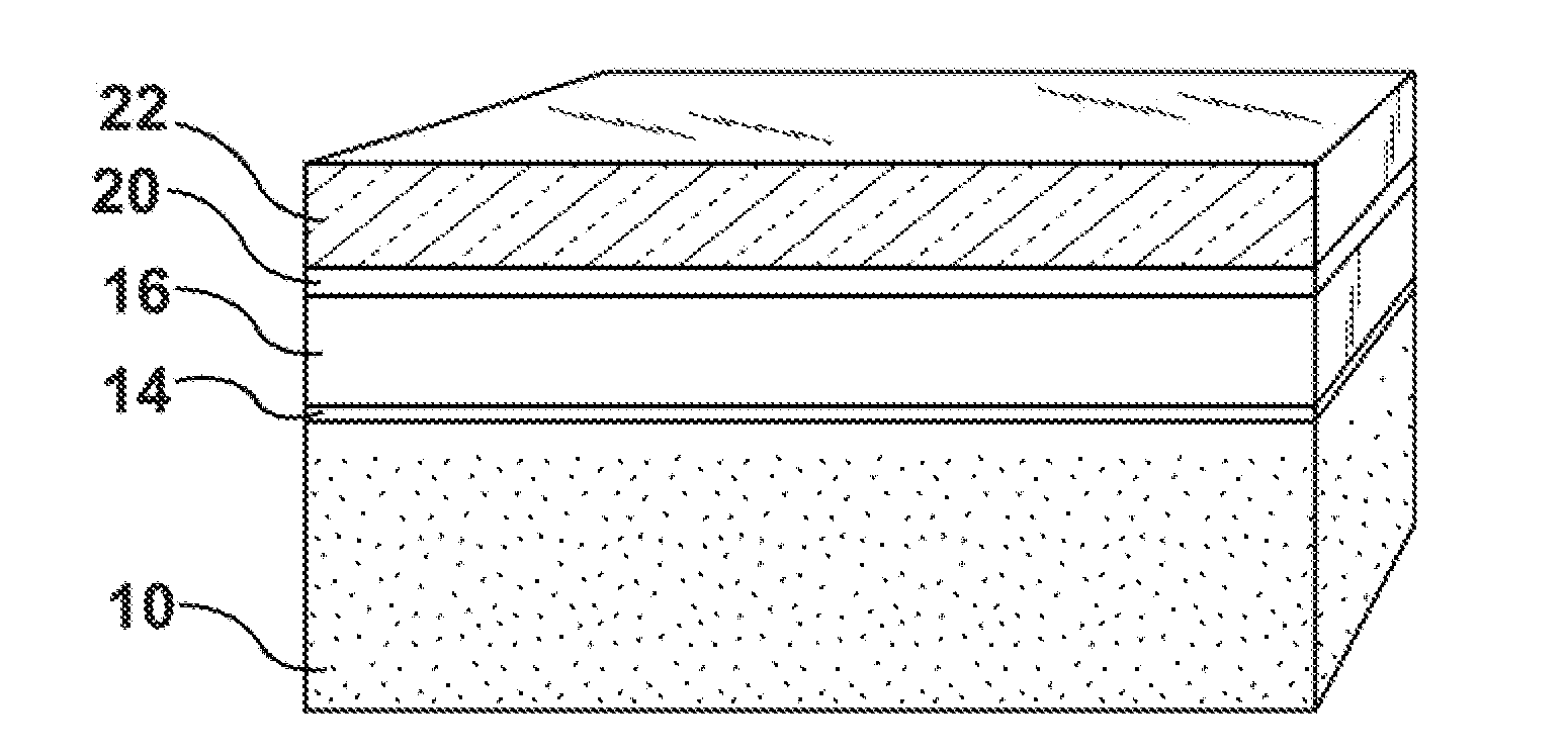
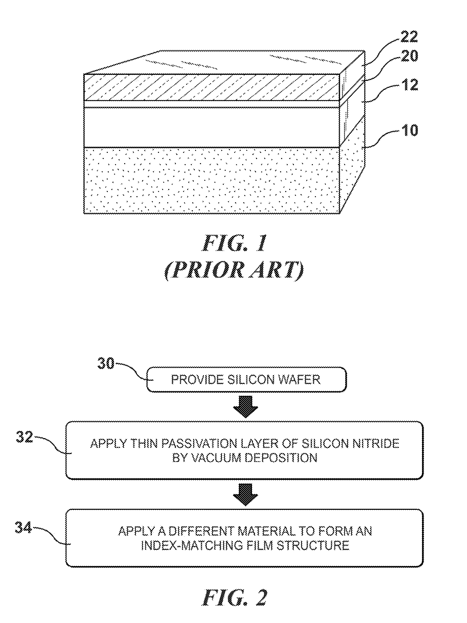
[0016]FIG. 1 shows a portion of a prior art silicon photovoltaic (“PV”) cell which is currently in widespread use. For clarity of explanation, the electrodes and p+or n−type doped regions are not shown. The PV cell includes a silicon semiconductor wafer 10, onto which various coatings or layers are applied. In a standard and widespread manufacturing technique, a single layer of silicon nitride 12 is applied onto a major (upper-shown) surface of wafer 10 for receiving photons. A standard technique for applying the silicon nitride layer 12 is by vacuum deposition, to a typical thickness of 1000 Angstrom. Thicknesses of layers as mentioned herein are average thicknesses, unless otherwise stated. Silicon nitride layer 12 functions to both passivate the surface of the silicon semiconductor wafer 10 that it overlies, as well as to reduce the reflectivity of the PV cell. Thus, in the prior art, the typically 1000-Angstrom thick silicon nitride layer 12 acts both as a passivation layer and ...


PUM

PropertyMeasurementUnit
thicknessaaaaaaaaaa
thicknessaaaaaaaaaa
thicknessesaaaaaaaaaa

Abstract

Disclosed is a method of passivating and reducing reflectance of a silicon photovoltaic cell. The method includes the step of providing a silicon wafer of a solar cell having a major surface. A passivation layer of silicon nitride is applied on at least 98 percent of the major surface through a vacuum deposition process. An index-matching film structure, different from silicon nitride, is applied on top of the passivation layer. The index matching film structure provides the majority of the antireflective property of the combination of the passivation layer and the index matching film structure.

Description

FIELD OF THE INVENTION[0001]The present invention relates to a method of applying various coatings or films on a silicon wafer in order to passivate the surface and reduce the reflectance of a photovoltaic cell.BACKGROUND OF THE INVENTION[0002]Silicon semiconductor wafers, or substrates, are widely used in the fabrication of photovoltaic (PV) cells capable of converting solar light to electrical energy. To maintain high performance PV device, a layer of material, such as silicon nitride, is typically applied to the surface of the silicon wafer to reduce the surface recombination of electrons and holes, also known in the art as “surface passivation”. Silicon nitride is preferred due to its good passivation properties and reasonable optical properties.[0003]In current silicon PV cell manufacturing, a widespread practice is to apply silicon nitride to a thickness of, typically, 1000 angstroms, which is more than the amount required to adequately passivate the silicon wafer. The relativ...

Claims


Application Information

Patent Timeline
Patent Type & Authority Applications(United States)
IPC IPC(8): H01L31/04H01L31/18
CPCY02E10/50H01L31/02168
Inventor TAKACS, LASZLO A.BUELOW, II, ROGER F.
Owner ENERGY FOCUS INC
Why Eureka
Try Eureka