Method and system for manufacturing a surface using character projection lithography with variable magnification

a character projection and variable magnification technology, applied in the field of lithography, can solve the problems of high computational cost, difficult to accurately translate the physical design to the actual circuit pattern developed on the resist layer, and difficult to add opc features,

Active Publication Date: 2011-02-24
D2S
View PDF6 Cites 23 Cited by
  • Summary
  • Abstract
  • Description
  • Claims
  • Application Information

AI Technical Summary

Benefits of technology

[0012]A character projection charged particle beam writer system is disclosed comprising a variab

Problems solved by technology

An example of an end-use limitation is defining the geometry of a transistor in a way in which it cannot sufficiently operate at the required supply voltage.
The design rule limitations reflect, among other things, the smallest dimensions that can be reliably fabricated.
As the critical dimensions of the circuit pattern become smaller and approach the resolution value of the exposure tool, the accurate transcription of the physical design to the actual circuit pattern developed on the resist layer becomes difficult.
Adding OPC features is a very laborious task, requires costly computation time, and results in more expensive reticles.
Not only are OPC patterns complex, but since optical proximity effects are long range compared to minimum line and space dimensions, the correct OPC patterns in a given location depend significantly on what other geometry is in the neighborhood.
There are numerous manufacturing factors that also cause variations, but the OPC component of that overall error is often in the range listed.
Since curvilinear patterns are difficult and expensive to form on

Method used


Image

  • Method and system for manufacturing a surface using character projection lithography with variable magnification
  • Method and system for manufacturing a surface using character projection lithography with variable magnification
  • Method and system for manufacturing a surface using character projection lithography with variable magnification

Examples


Embodiment Construction

[0029]The improvements and advantages of the present disclosure can be accomplished by use of a charged particle beam writer system in which the de-magnification can be adjusted for each shot, and by creating and using a shot list which contains a magnification for each shot.

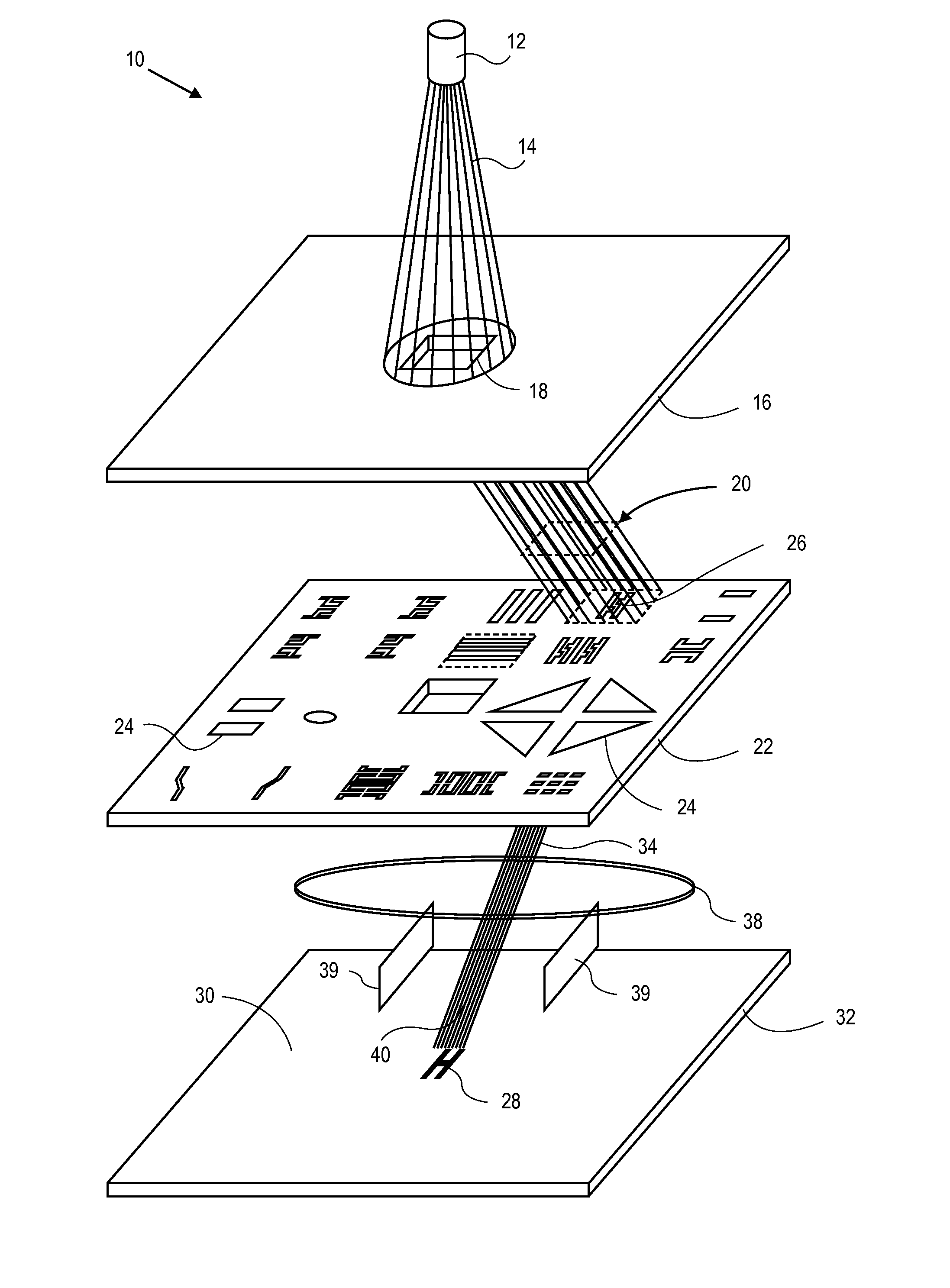
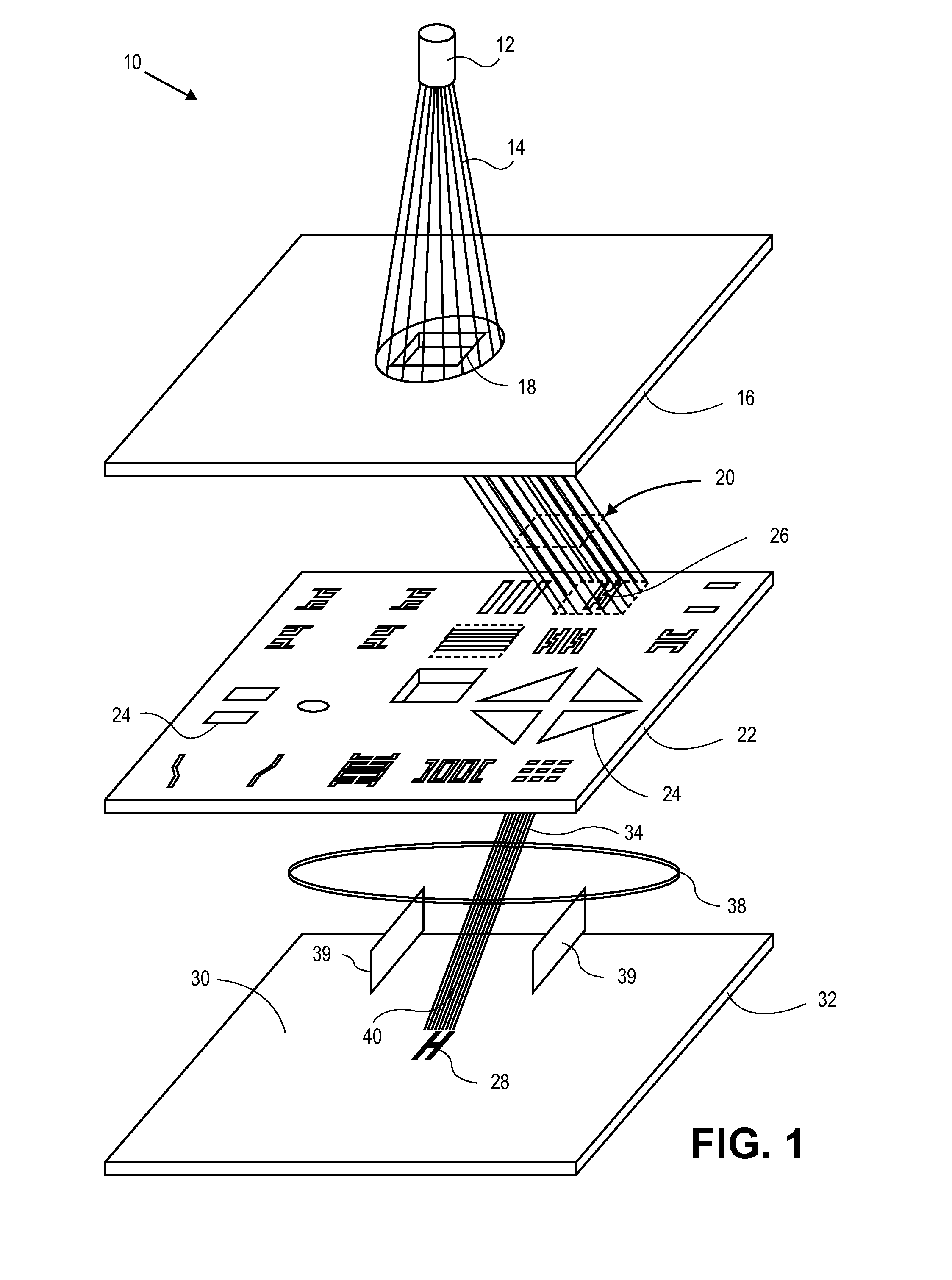
[0030]Referring now to the drawings, wherein like numbers refer to like items, number 10 identifies an embodiment of a lithography system, such as a particle beam writer system, in this case an electron beam writer system, that employs character projection to manufacture a surface 30. The electron beam writer system 10 has an electron beam source 12 that projects an electron beam 14 toward an aperture plate 16. The plate 16 has an aperture 18 formed therein which allows the electron beam 14 to pass. Once the electron beam 14 passes through the aperture 18 it is directed or deflected by a system of lenses (not shown) as electron beam 20 toward another rectangular aperture plate or stencil mask 22. The stencil 22 ...


PUM


Abstract

A character projection charged particle beam writer system is disclosed comprising a variable magnification reduction lens which will allow different shot magnifications on a shot by shot basis. A method for fracturing or mask data preparation or optical proximity correction is also disclosed comprising assigning a magnification to each calculated charged particle beam writer shot. A method for forming a pattern on a surface is also disclosed comprising using a charged particle beam writer system and varying the magnification from shot to shot. A method for manufacturing an integrated circuit using optical lithography is also disclosed, comprising using a charged particle beam writer system to form a pattern on a reticle, and varying the magnification of the charged particle beam writer system from shot to shot.

Description

RELATED APPLICATIONS[0001]This application claims priority from U.S. Provisional Patent Application Ser. No. 61 / 236,050, filed Aug. 21, 2009, entitled “Method and System For Manufacturing a Surface Having Variable Sized Patterns Using Character Projection Lithography”; which is hereby incorporated by reference for all purposes.BACKGROUND OF THE DISCLOSURE[0002]The present disclosure is related to lithography, and more particularly to the design of a charged particle beam writer system and methods for using the charged particle beam writer system to manufacture a surface which may be a reticle, a wafer, or any other surface.[0003]In the production or manufacturing of semiconductor devices, such as integrated circuits, optical lithography may be used to fabricate the semiconductor devices. Optical lithography is a printing process in which a lithographic mask or photomask manufactured from a reticle is used to transfer patterns to a substrate such as a semiconductor or silicon wafer t...

Claims


Application Information

Patent Timeline
IPC IPC(8): G03F7/20G03B27/52G06F17/50
CPCB82Y10/00B82Y40/00G03F7/2061Y10S430/143G03F1/20G03F7/2047H01J37/3174
Inventor FUJIMURA, AKIRA
Owner D2S
Why Eureka
Try Eureka