Nitride semiconductor element, methods for manufacturing nitride semiconductor element and nitride semiconductor layer, and nitride semiconductor light-emitting element

a technology of nitride semiconductor and semiconductor layer, which is applied in the direction of semiconductor/solid-state device manufacturing, semiconductor devices, electrical devices, etc., can solve the problems of threading dislocation propagation, inability to effectively reduce the dislocation density of the gan semiconductor layer corresponding to the topmost layer, and inability to prevent threading dislocation propagation. , to achieve the effect of excellent surface flatness and improved crystallinity

Active Publication Date: 2011-03-03
SHARP FUKUYAMA LASER CO LTD
View PDF5 Cites 29 Cited by
  • Summary
  • Abstract
  • Description
  • Claims
  • Application Information

AI Technical Summary

Benefits of technology

[0041]Furthermore, according to the present invention, a method for manufacturing a nitride semiconductor layer exhibiting excellent surface flatness while allowing improvement in crystallinity can be provided.

Problems solved by technology

However, when threading dislocation occurs in the underlying GaN semiconductor layer exposed through the opening of the SiN layer, propagation of the threading dislocation cannot be prevented by the SiN layer, which causes the threading dislocation to propagate also to the GaN semiconductor layer on the SiN layer.
This poses a problem that the dislocation density in the GaN semiconductor layer corresponding to the topmost layer cannot be effectively decreased.
In addition, in the case where the opening in the surface of the SiN layer is reduced in area and the SiN layer in the surface of the sapphire substrate is increased in coverage rate, there is a problem that the flatness of the surface of the GaN semiconductor layer corresponding to the topmost layer may be deteriorated.

Method used


Image

  • Nitride semiconductor element, methods for manufacturing nitride semiconductor element and nitride semiconductor layer, and nitride semiconductor light-emitting element
  • Nitride semiconductor element, methods for manufacturing nitride semiconductor element and nitride semiconductor layer, and nitride semiconductor light-emitting element
  • Nitride semiconductor element, methods for manufacturing nitride semiconductor element and nitride semiconductor layer, and nitride semiconductor light-emitting element

Examples


first embodiment

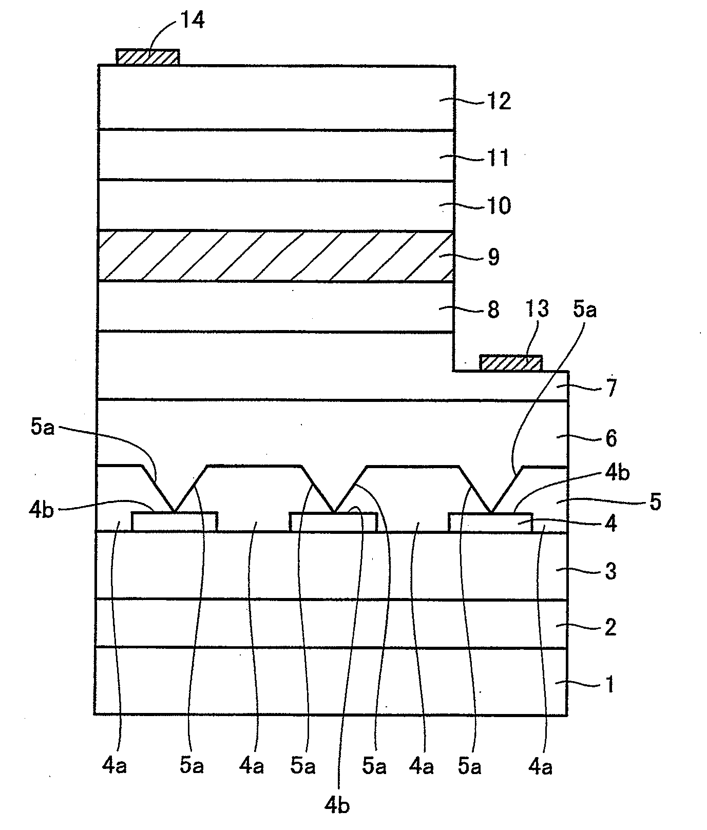
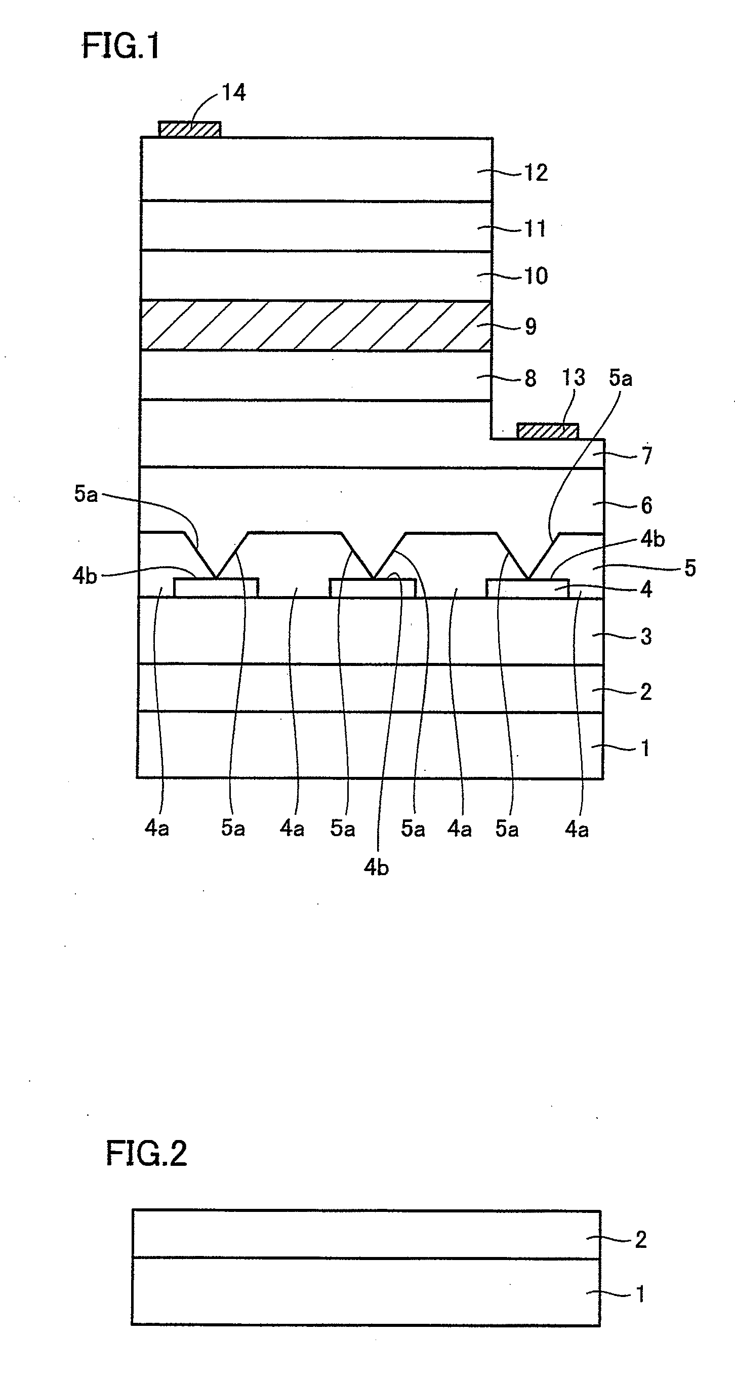
[0073]FIG. 1 is a schematic cross sectional view of a nitride semiconductor light-emitting diode element according to the first embodiment which is an example of the nitride semiconductor element of the present invention.

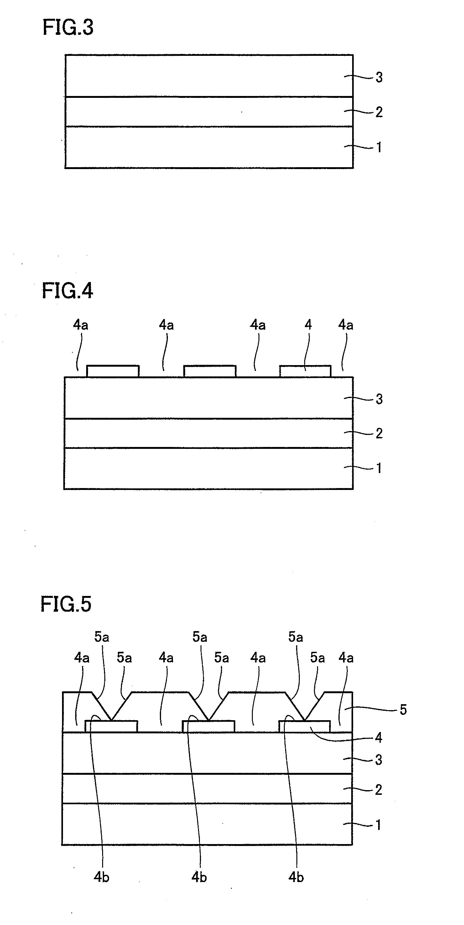
[0074]The nitride semiconductor light-emitting diode element according to the first embodiment includes a substrate 1; a nitride semiconductor buffer layer 2 provided in contact with the surface of substrate 1; a nitride semiconductor underlying layer 3 provided in contact with the surface of nitride semiconductor buffer layer 2; a silicon nitride layer 4 having an opening 4a and provided in contact with the surface of nitride semiconductor underlying layer 3; a first nitride semiconductor layer 5 provided in contact with the surface of silicon nitride layer 4 and extending through opening 4a of silicon nitride layer 4; a second nitride semiconductor layer 6 provided in contact with the surface of first nitride semiconductor layer 5; an n-type nitride semiconductor ...

second embodiment

[0126]The present embodiment is characterized in that nitride semiconductor buffer layer 2 is stacked not by the MOCVD method but by the sputtering method.

[0127]In this case, nitride semiconductor buffer layer 2 may be provided, for example, by stacking a nitride semiconductor layer formed of a nitride semiconductor represented by an expression Alx1Ga1-x1N (0x1Ga1-x1N (0.5≦x1≦1) in which the atomic ratio of Al is 0.5 or more. It is more preferable that the nitride semiconductor layer made of AlN is stacked by the sputtering method. When nitride semiconductor buffer layer 2 is provided by stacking, by the sputtering method, a nitride semiconductor layer formed of a nitride semiconductor represented by an expression Alx1Ga1-x1N (0.5≦x1≦1) in which the atomic ratio of Al is 0.5 or more, particularly when the nitride semiconductor layer made of AlN is stacked by the sputtering method, it becomes possible to stack nitride semiconductor buffer layer 2 formed of an aggregate of columnar cr...

third embodiment

[0142]The present embodiment is characterized in that not a nitride semiconductor light-emitting diode element but a nitride semiconductor laser element is fabricated.

[0143]FIG. 13 is a schematic cross sectional view of a nitride semiconductor laser element according to the third embodiment which is another example of the nitride semiconductor element of the present invention.

[0144]In the nitride semiconductor laser element according to the third embodiment, on the surface of substrate 1, nitride semiconductor buffer layer 2, nitride semiconductor underlying layer 3, silicon nitride layer 4, first nitride semiconductor layer 5, second nitride semiconductor layer 6, an n-type nitride semiconductor clad layer 21, an n-type nitride semiconductor light guide layer 22, a nitride semiconductor active layer 23, a nitride semiconductor protection layer 24, a p-type nitride semiconductor light guide layer 25, a p-type nitride semiconductor clad layer 26, and a p-type nitride semiconductor co...


PUM

PropertyMeasurementUnit
angleaaaaaaaaaa
angleaaaaaaaaaa
pressureaaaaaaaaaa

Abstract

Described herein is a method for manufacturing a nitride semiconductor layer by stacking, on a silicon nitride layer, the first nitride semiconductor layer having a surface inclined with respect to the surface of the silicon nitride layer and then stacking the second nitride semiconductor layer on the first nitride semiconductor layer, a nitride semiconductor element and a nitride semiconductor light-emitting element each including the nitride semiconductor layer; and a method for manufacturing the nitride semiconductor element.

Description

[0001]This nonprovisional application is based on Japanese Patent Application No. 2009-201602 filed on Sep. 1, 2009 and No. 2010-134988 filed on Jun. 14, 2010, with the Japan Patent Office, the entire contents of which are hereby incorporated by reference.BACKGROUND OF THE INVENTION[0002]1. Field of the Invention[0003]The present invention relates to a nitride semiconductor element such as a light-emitting device including a nitride semiconductor light-emitting diode element, a nitride semiconductor laser element and the like and an electronic device including a nitride semiconductor transistor element and the like; a method for manufacturing the nitride semiconductor element; a method for manufacturing a nitride semiconductor layer; and a nitride semiconductor light-emitting element.[0004]2. Description of the Background Art[0005]Conventionally, a GaN substrate, an SiC substrate, a sapphire substrate, and the like are used as a substrate used for a nitride semiconductor element. Fr...

Claims


Application Information

Patent Timeline
Patent Type & Authority Applications(United States)
IPC IPC(8): H01L33/02H01L29/12H01L21/18
CPCH01L21/0242H01L21/02433H01L21/02458H01L21/02505H01L21/0254H01L21/02639H01L33/325H01L29/2003H01L29/66462H01L29/7787H01L33/16H01L33/22H01L21/02647
Inventor KOMADA, SATOSHI
Owner SHARP FUKUYAMA LASER CO LTD
Why Eureka
Try Eureka