Semiconductor device, method for fabricating the same, and plasma doping system

a semiconductor device and plasma doping technology, applied in the direction of transistors, chemical vapor deposition coatings, coatings, etc., can solve the problems of inability to obtain desired transistor characteristics, so as to reduce the process time

Active Publication Date: 2011-03-03
SAMSUNG ELECTRONICS CO LTD
View PDF14 Cites 11 Cited by
  • Summary
  • Abstract
  • Description
  • Claims
  • Application Information

AI Technical Summary

Problems solved by technology

As a result, the problem arises that desired transistor characteristics cannot be obtained.

Method used


Image

  • Semiconductor device, method for fabricating the same, and plasma doping system
  • Semiconductor device, method for fabricating the same, and plasma doping system
  • Semiconductor device, method for fabricating the same, and plasma doping system

Examples


example embodiment 1

[0081]A semiconductor device according to the first example embodiment of the present disclosure and a method for fabricating the same will be described with reference to the drawings.

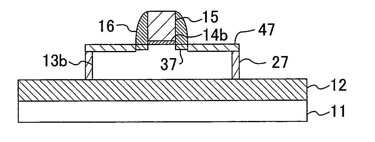
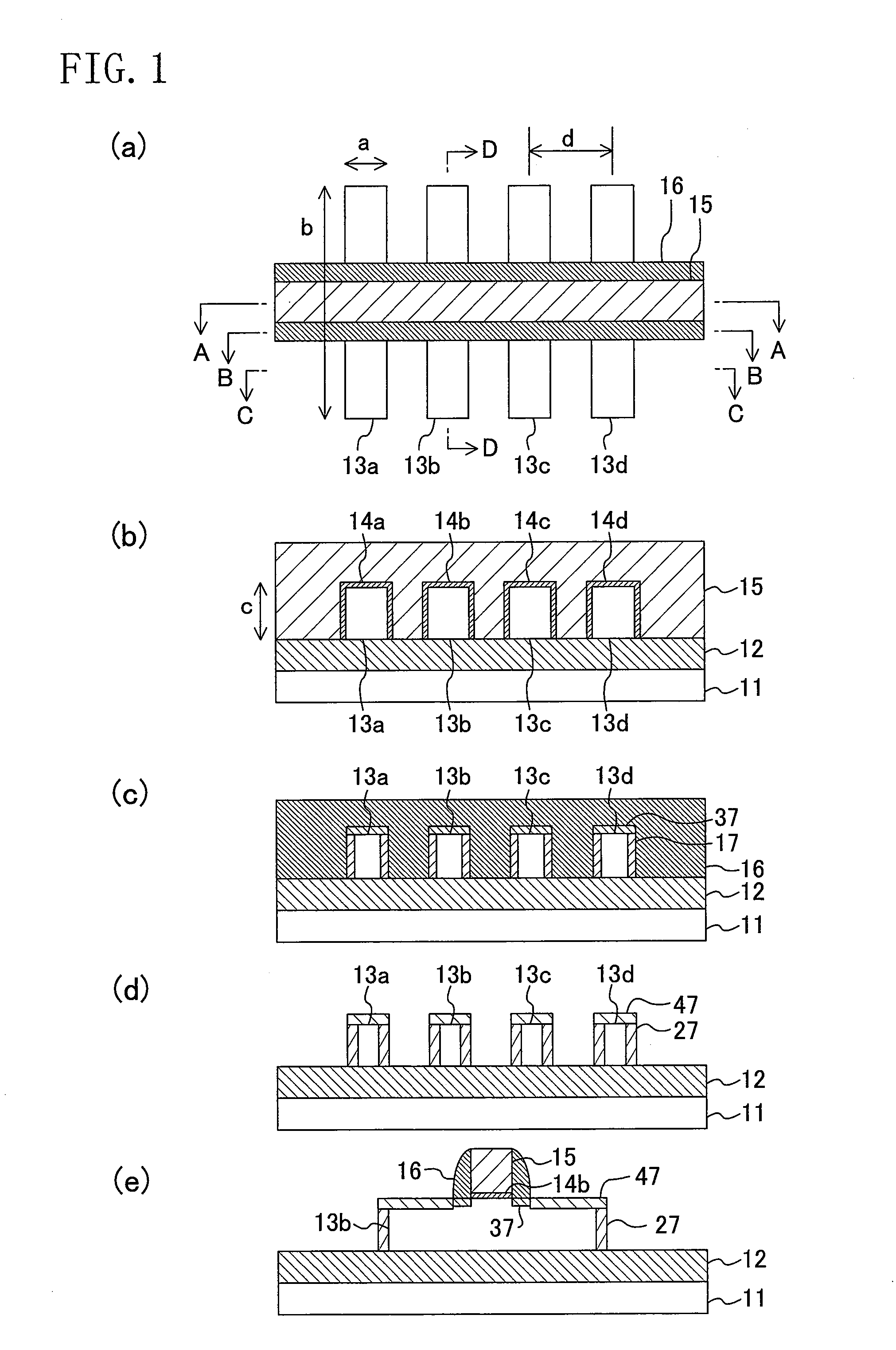
[0082]FIGS. 1(a)-1(e) are views each showing a structure of the semiconductor device according to the present example embodiment, specifically the semiconductor device having a fin-FET, of which FIG. 1(a) is a plan view, FIG. 1(b) is a cross-sectional view along the line A-A in FIG. 1(a), FIG. 1(c) is a cross-sectional view along the line B-B in FIG. 1(a), FIG. 1(d) is a cross-sectional view along the line C-C in FIG. 1(a), and FIG. 1(e) is a cross-sectional view along the line D-D in FIG. 1(a).

[0083]As shown in FIGS. 1(a)-1(e), the fin-FET according to the present example embodiment has a support substrate 11 made of, e.g., silicon, an insulating layer 12 made of, e.g., silicon dioxide formed on the support substrate 11, fin-semiconductor regions 13a-13d formed on the insulating layer 12 and made of, ...

example embodiment 2

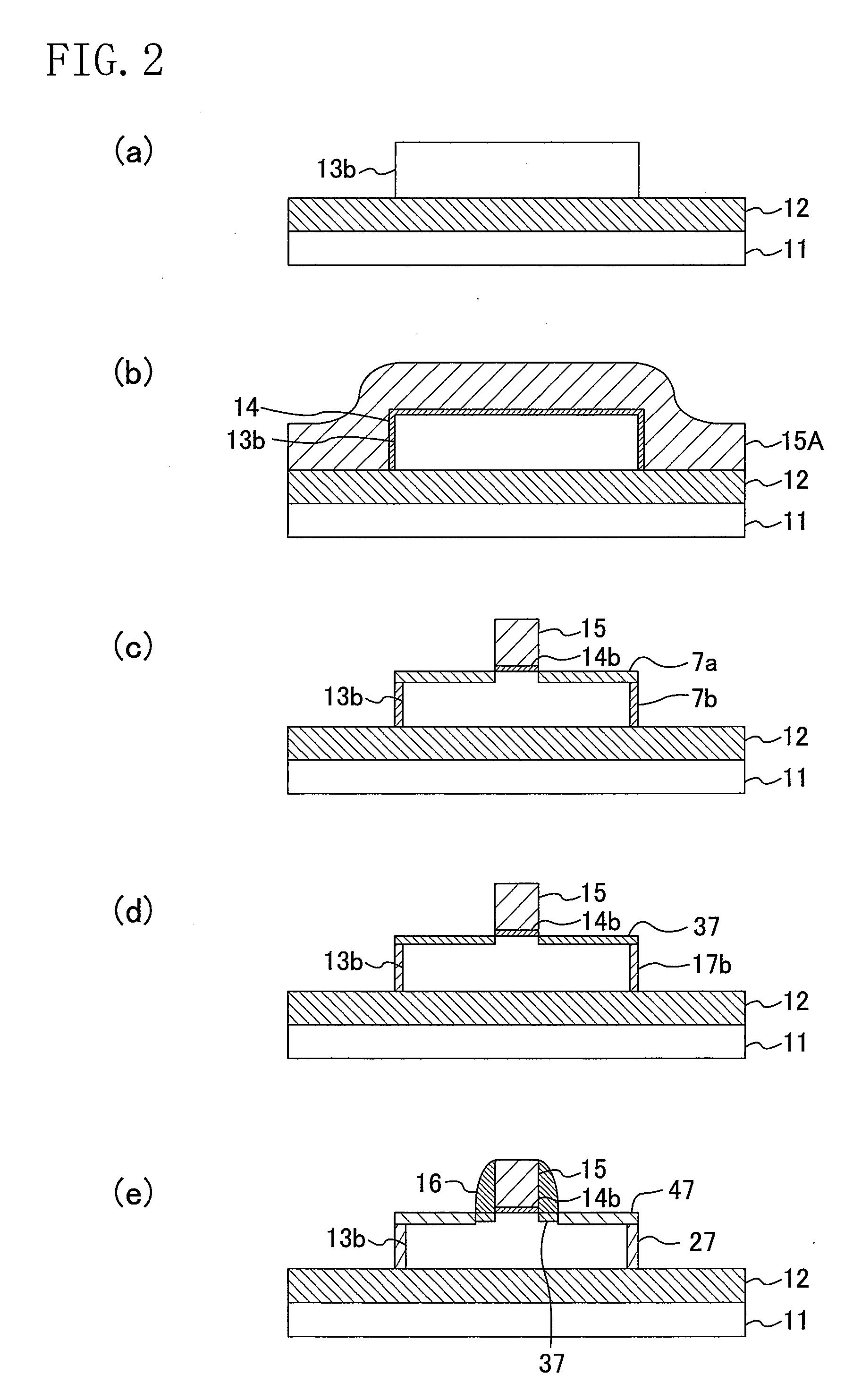
[0118]A semiconductor device according to the second example embodiment of the present disclosure and a method for fabricating the same will be described with reference to the drawings.

[0119]The semiconductor device according to the present example embodiment, specifically the semiconductor device having a fin-FET has the same two-dimensional structure as the two-dimensional structure of the semiconductor device according to the first example embodiment shown in FIG. 1(a). FIGS. 4(a)-4(c) are views each showing a structure of the semiconductor device according to the present example embodiment, specifically the semiconductor device having the fin-FET, of which FIG. 4(a) is a cross-sectional view along the line B-B in FIG. 1(a), FIG. 4(b) is a cross-sectional view along the line C-C in FIG. 1(a), and FIG. 4(c) is a cross-sectional view along the line D-D in FIG. 1(a). Note that, in the present example embodiment, the cross-sectional structure along the line A-A in FIG. 1(a) is the sa...


PUM

PropertyMeasurementUnit
thicknessaaaaaaaaaa
heightaaaaaaaaaa
widthaaaaaaaaaa

Abstract

A fin-semiconductor region (13) is formed on a substrate (11). A first impurity which produces a donor level or an acceptor level in a semiconductor is introduced in an upper portion and side portions of the fin-semiconductor region (13), and oxygen or nitrogen is further introduced as a second impurity in the upper portion and side portions of the fin-semiconductor region (13).

Description

TECHNICAL FIELD[0001]The present disclosure relates to a semiconductor device, a method for fabricating the same, and a plasma doping system, and particularly to a semiconductor device of a three-dimensional structure having a fin-type semiconductor region on a substrate, and a method for fabricating the same.BACKGROUND ART[0002]In recent years, as semiconductor devices have become higher in integration, functionality, and speed, demand for miniaturization of the semiconductor devices has been growing. To satisfy the demand, various device structures have been proposed for reducing the area occupied by transistors over a substrate. Among them, a field effect transistor having a fin-type structure has drawn attention. The field effect transistor having the fin-type structure is generally called a fin-FET (Fin-Field Effect Transistor), and has an active region made of a semiconductor region (hereinafter referred to as a fin-semiconductor region) having a thin-wall (fin) shape perpendi...

Claims


Application Information

Patent Timeline
Patent Type & Authority Applications(United States)
IPC IPC(8): H01L29/786H01L21/336H01L21/425H01L21/465
CPCH01L21/2236H01L29/785H01L29/66803
Inventor OKUMURA, TOMOHIROKAI, TAKAYUKISASAKI, YUICHIRO
Owner SAMSUNG ELECTRONICS CO LTD
Why Eureka
Try Eureka