

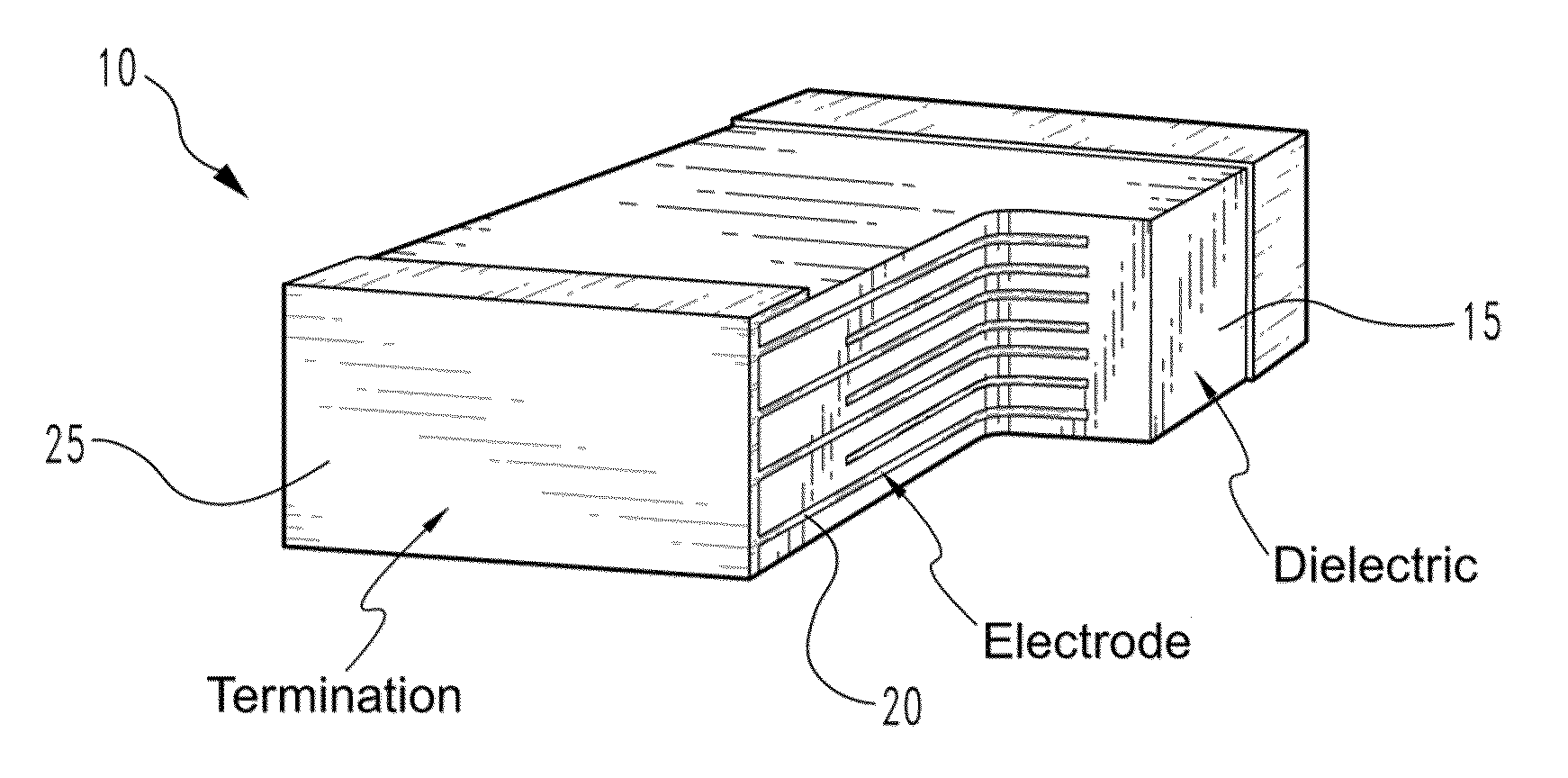
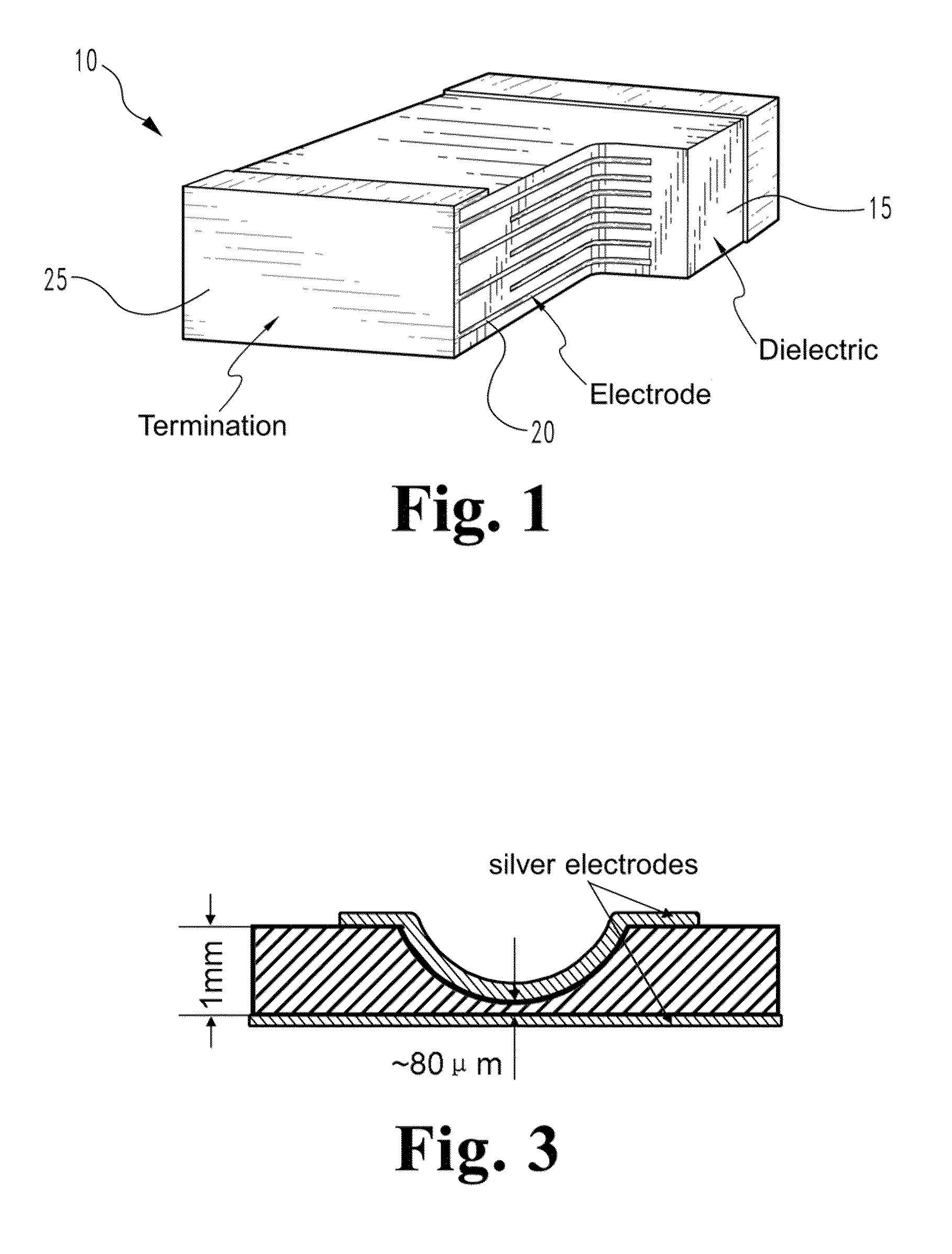
Nanostructured dielectric materials for high energy density multi layer ceramic capacitors
a ceramic capacitor and nanostructured dielectric technology, applied in the field of ceramic science, can solve the problems of high dielectric loss and lower resistivity of devices, and achieve the effect of high energy density capacitors
- Summary
- Abstract
- Description
- Claims
- Application Information
AI Technical Summary
Benefits of technology
Problems solved by technology
Method used
Image

Examples
examples
I Microstructural Developments and General Testing Conditions
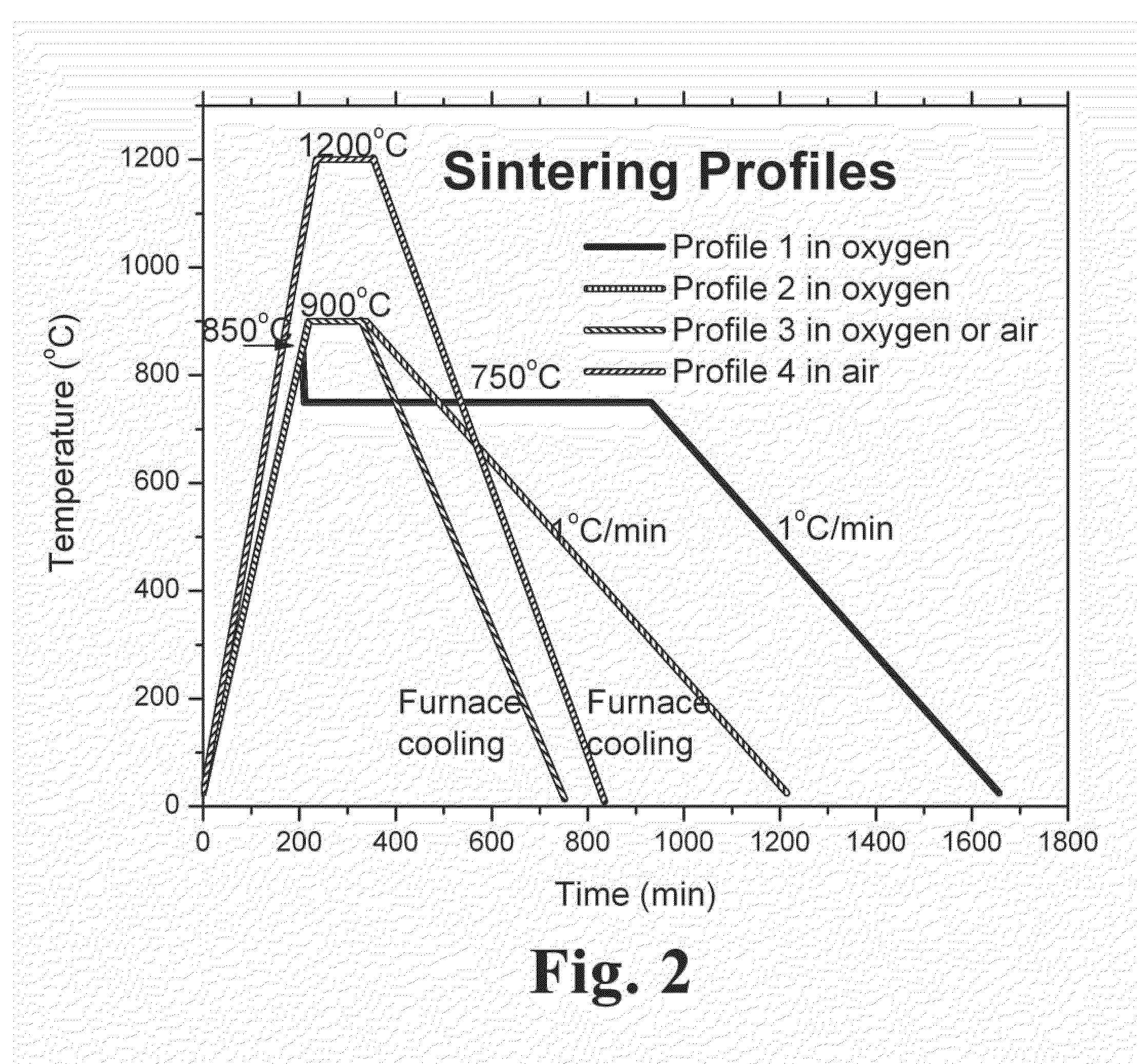
[0036]NANOTEK® TiO2 powders were obtained as starting materials for MLCC production, with powder characteristics and main impurity levels reproduced from the included product data sheet as Tables 1 and 2, respectively (NANOTEK is a registered trademark of Nanophase Technologies Corporation, 1319 Marquette Drive, Romeoville, Ill., 60446, Reg. No. 1978354). Green compacts were prepared by uniaxial pressing at 50 MPa and subsequent cold isostatic pressing at 300 MPa. Sintering was conducted at various temperatures (750° C.-1200° C.) in pure oxygen (1 atm.) or air with different cooling rates (furnace cooling or 1° C. / min cooling rate).
TABLE 1Characteristics of the starting powdersCharacteristicsValuePurity99.9%Average particle size (nm)40Specific surface area (m2 / g)38Bulk density (g / cm3)0.20True density (g / cm3)3.95Crystal phase80% anatase and 20% rutile
TABLE 2Main impurities in the TiO2 powderElementsImpurity level (%)Fe0.037...
PUM
| Property | Measurement | Unit |
|---|---|---|
| Grain size | aaaaa | aaaaa |
| Grain size | aaaaa | aaaaa |
| Grain size | aaaaa | aaaaa |
Abstract
Description
Claims
Application Information