Single-crystal manufacturing apparatus and single-crystal manufacturing method
a manufacturing apparatus and single crystal technology, applied in the direction of polycrystalline material growth, crystal growth process, protective fluid, etc., can solve the problems of insufficient cooling efficiency and decrease in cooling efficiency of crystals, and achieve enhanced cooling effect of single crystal during pulling, a higher growth rate, and a larger temperature gradient in crystals
- Summary
- Abstract
- Description
- Claims
- Application Information
AI Technical Summary
Benefits of technology
Problems solved by technology
Method used
Image
Examples
example 1
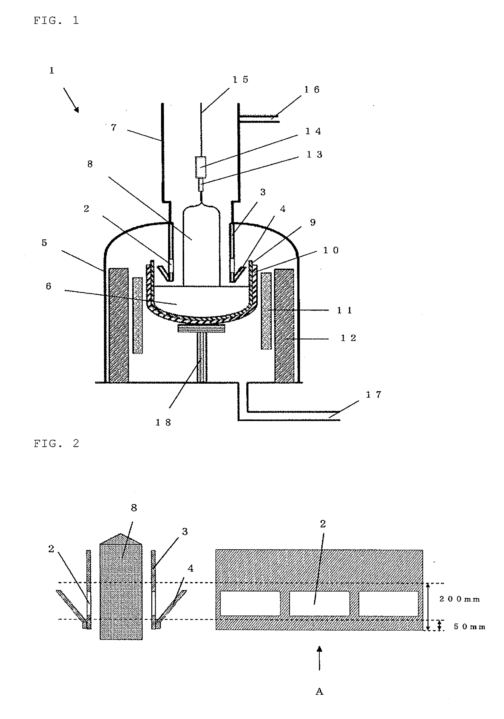
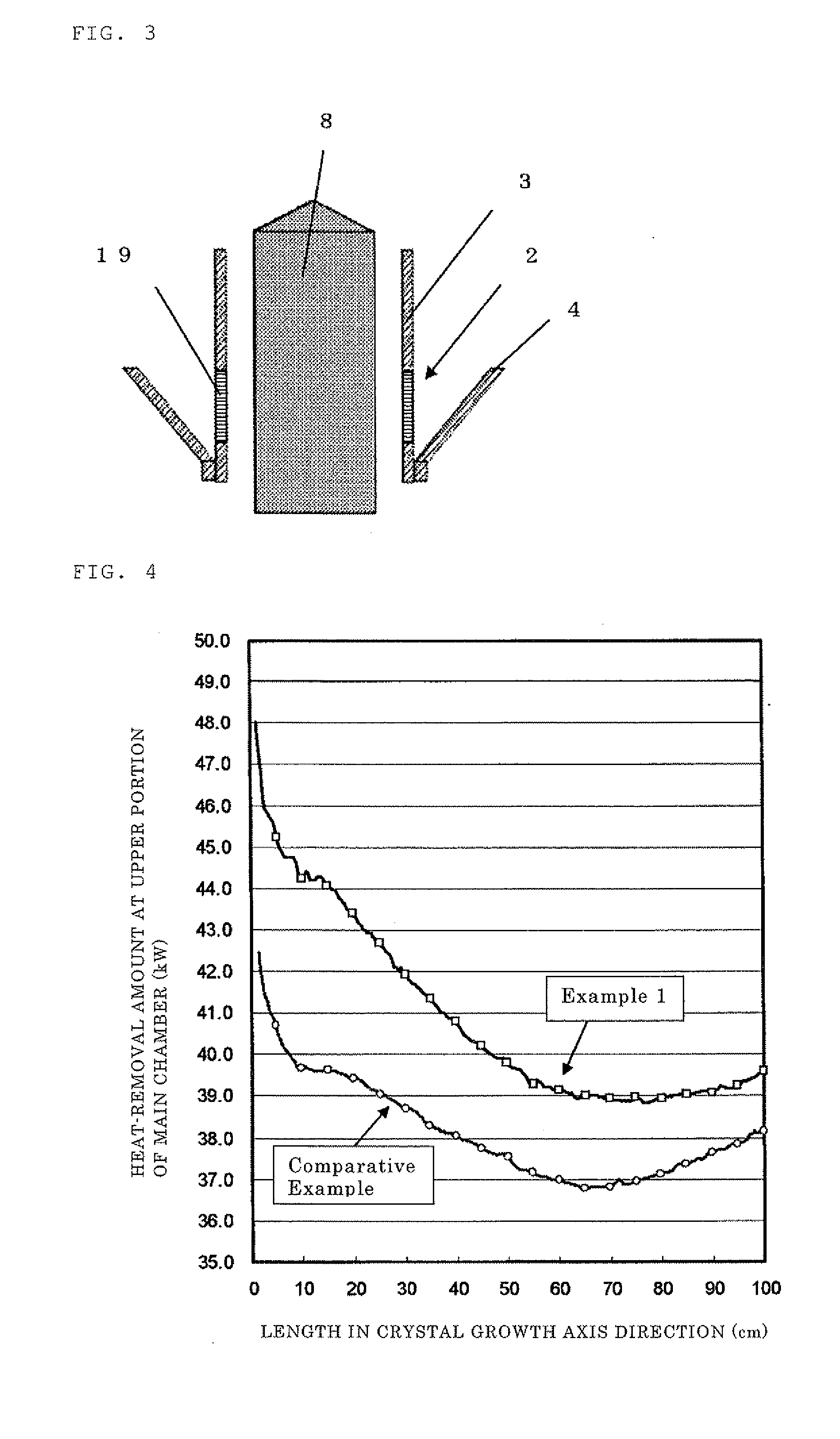
[0066]The single-crystal manufacturing apparatus according to the present invention as shown in FIG. 1 was used to manufacture a N-region silicon single crystal having a diameter of 200 mm. The heat-removal amount at the upper portion of the main chamber and the manufacture time were evaluated.
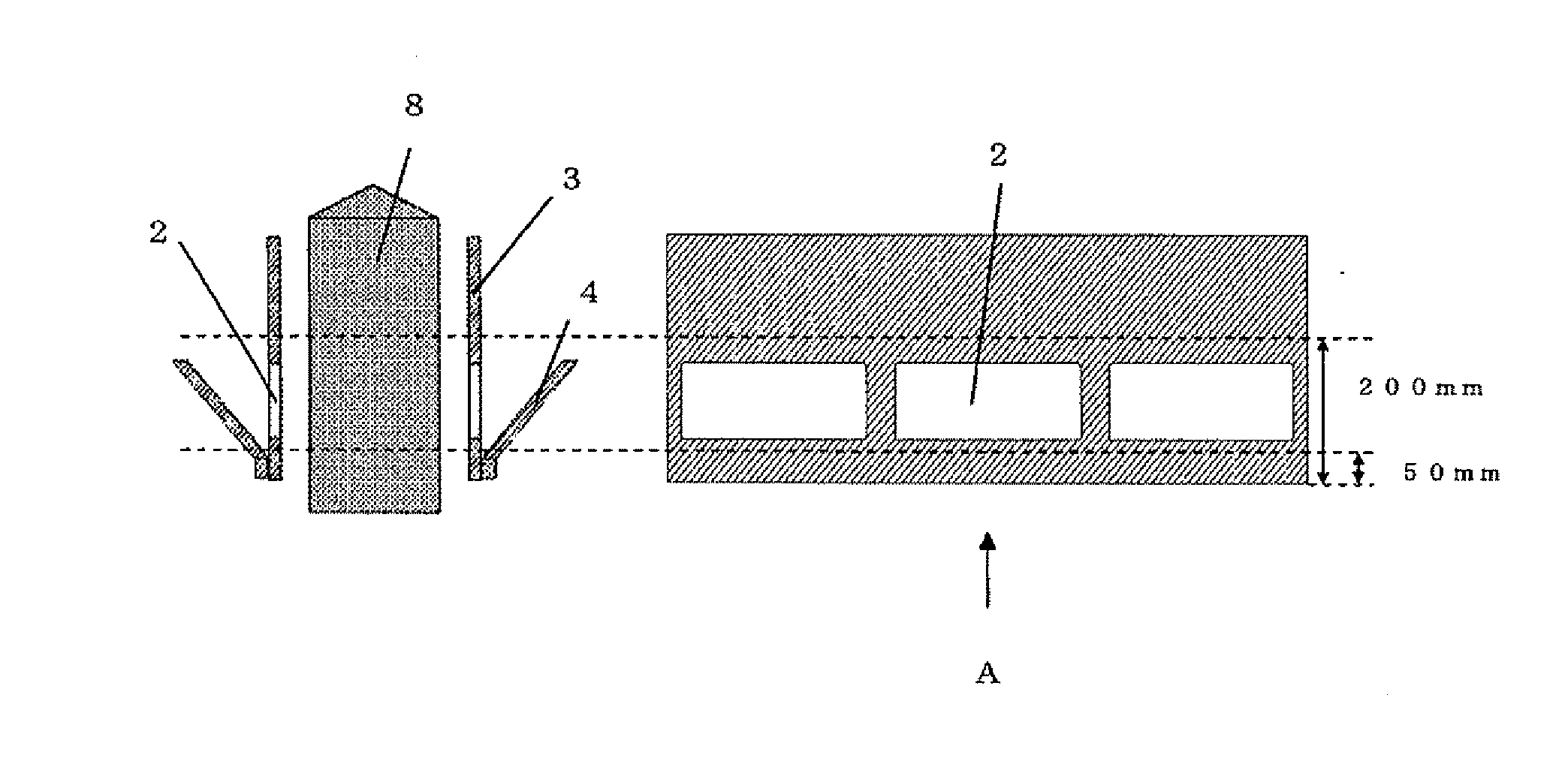
[0067]The crucible having a diameter of 650 mm was used. Three windows as shown in FIG. 2 was provided in the region between 50 and 200 mm from the lower end of the gas flow-guide cylinder. A ratio of the opening area thereof to the surface area of the region between 50 and 200 mm was 72%. The distance between the lower end of the gas flow-guide cylinder and the surface of the melt was 50 mm.
[0068]First, a polycrystalline silicon raw material with high purity having a weight of 180 kg was charged into the crucible and was heated to a temperature of a melting point (approximately 1420° C.) or more to be the melt. The single crystal was grown with controlling the V / G value during pulling so as t...
example 2
[0075]With the same single-crystal manufacturing apparatus as Example 1 except that the distance between the lower end of the gas flow-guide cylinder and the surface of the melt was 58 mm, the growth rate was gradually decreased during the pulling as with Example 1, and defect distribution of the obtained single crystal was evaluated.
[0076]The result is shown in FIG. 5. As shown in FIG. 5, it was revealed that although the growth rate was somewhat lower than Example 1, the growth rate at which N-region can obtain was higher than that of the later-described Comparative Example. For example, with regard to N-region right below an OSF region at the vicinity of a center axis of the crystal, the growth rate of Example 2 was improved by 12% as compared with that of Comparative Example.
[0077]In comparison with the result of Example 1, it was revealed that with regard to a range of the growth rate at which all parts in a crystal diameter can become N-region (a range of A in the figure), Exa...
PUM
 Abstract
Description
Claims
Application Information


