Light-Emitting Element, Light-Emitting Device, Lighting Device, and Electronic Device

Active Publication Date: 2011-03-10
SEMICON ENERGY LAB CO LTD
View PDF38 Cites 30 Cited by
  • Summary
  • Abstract
  • Description
  • Claims
  • Application Information

AI Technical Summary

Benefits of technology

[0019]A light-emitting element which has a plurality of light-emitting layers and can be driven at low voltage can be provided. In addition, loss of light extraction efficiency due to absorption of emitted light can be reduced; thus, a light-emitting element with high luminous efficiency can be provided.
[0020]Furthermore, by manufacture of a

Problems solved by technology

However, in the light-emitting element having such a structure, mutual interaction occurs between the metal-doped layer and the charge-generation layer formed of the oxide at their interface and the interface has a high electric field; thus, high voltage is needed for driving the light-emitting element, unfortunately.
There is a problem in that if a layer which has a peak of an absorption spectrum in a wavelength range of 400 nm t

Method used


Image

  • Light-Emitting Element, Light-Emitting Device, Lighting Device, and Electronic Device
  • Light-Emitting Element, Light-Emitting Device, Lighting Device, and Electronic Device
  • Light-Emitting Element, Light-Emitting Device, Lighting Device, and Electronic Device

Examples


embodiment 1

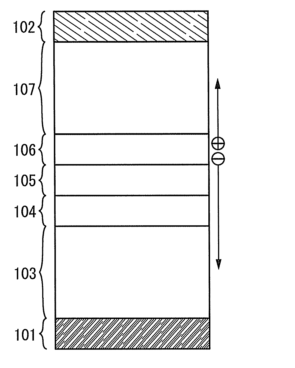
[0042]In Embodiment 1, one embodiment of a light-emitting element will be described with reference to FIGS. 1A and 1B.

[0043]In an element structure illustrated in FIG. 1A, a first EL layer 103 and a second EL layer 107 each including a light-emitting region are interposed between a pair of electrodes (i.e., an anode 101 and a cathode 102), and between the first EL layer 103 and the second EL layer 107, an electron-injection buffer 104, an electron-relay layer 105, and a charge-generation layer 106 are stacked in this order over the anode 101.

[0044]The charge-generation layer 106 is a layer containing a substance having high hole-transport properties and an acceptor substance, where holes and electrons that are carriers of the light-emitting element are generated. The holes generated in the charge-generation layer 106 move to the second EL layer 107 while the electrons move to the electron-relay layer 105. Moreover, since the electron-relay layer 105 has high electron-transport prope...

embodiment 2

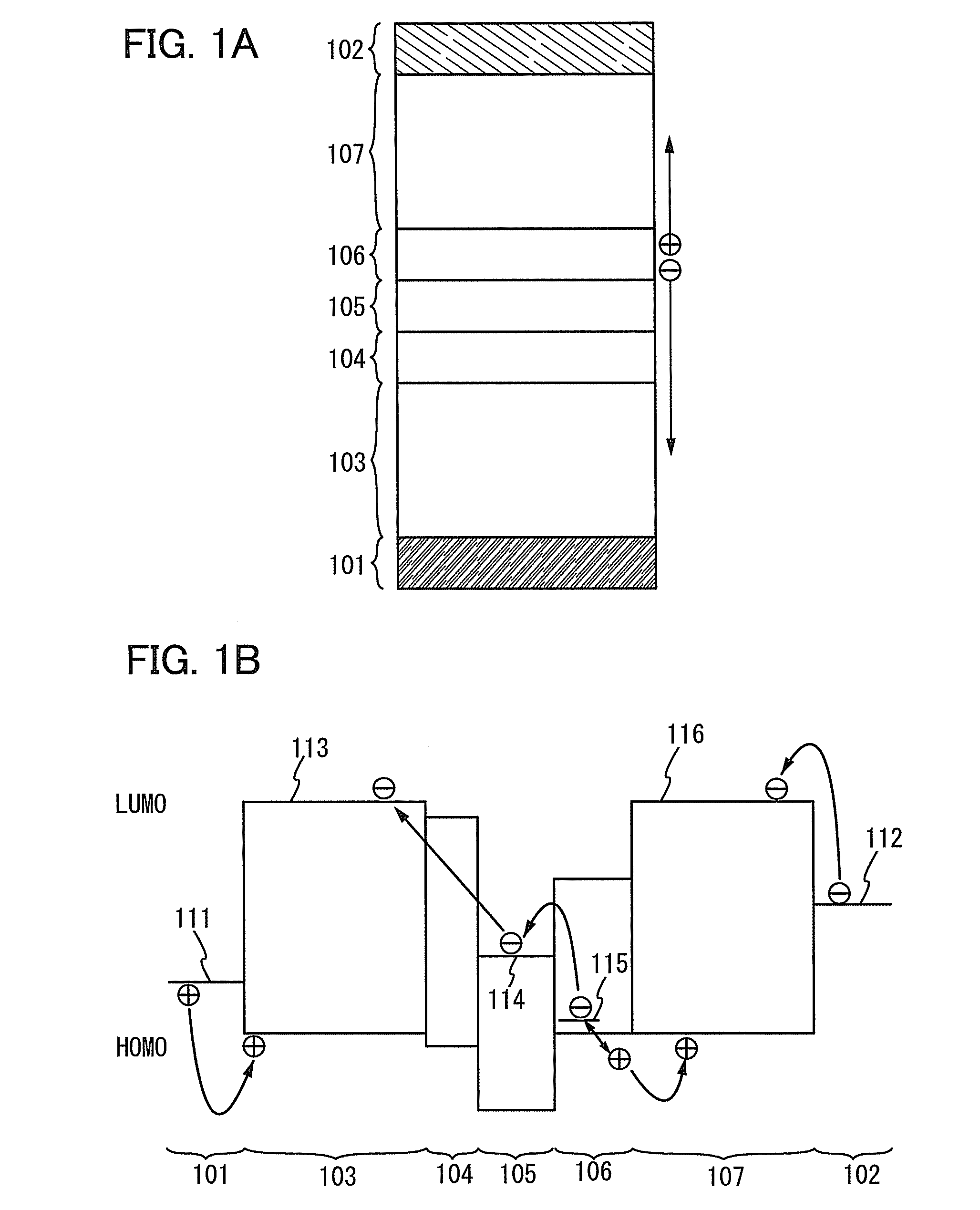
[0104]In Embodiment 2, an example of the light-emitting element included in the basic structure described in Embodiment 1 will be described with reference to FIGS. 2A and 2B. Specifically, a case where the electron-injection buffer 104 in the light-emitting element described in Embodiment 1 has a single layer of an alkali metal, an alkaline earth metal, a rare earth metal, or a compound thereof will be described.

[0105]As illustrated in FIG. 2A, in a light-emitting element described in this embodiment, the first EL layer 103 and the second EL layer 107 each including a light-emitting region are interposed between a pair of electrodes (i.e., the anode 101 and the cathode 102), and between the first EL layer 103 and the second EL layer 107, the electron-injection buffer 104, the electron-relay layer 105, and the charge-generation layer 106 are stacked in this order over the anode 101.

[0106]The anode 101, the cathode 102, the first EL layer 103, the second EL layer 107, the charge-gener...

embodiment 3

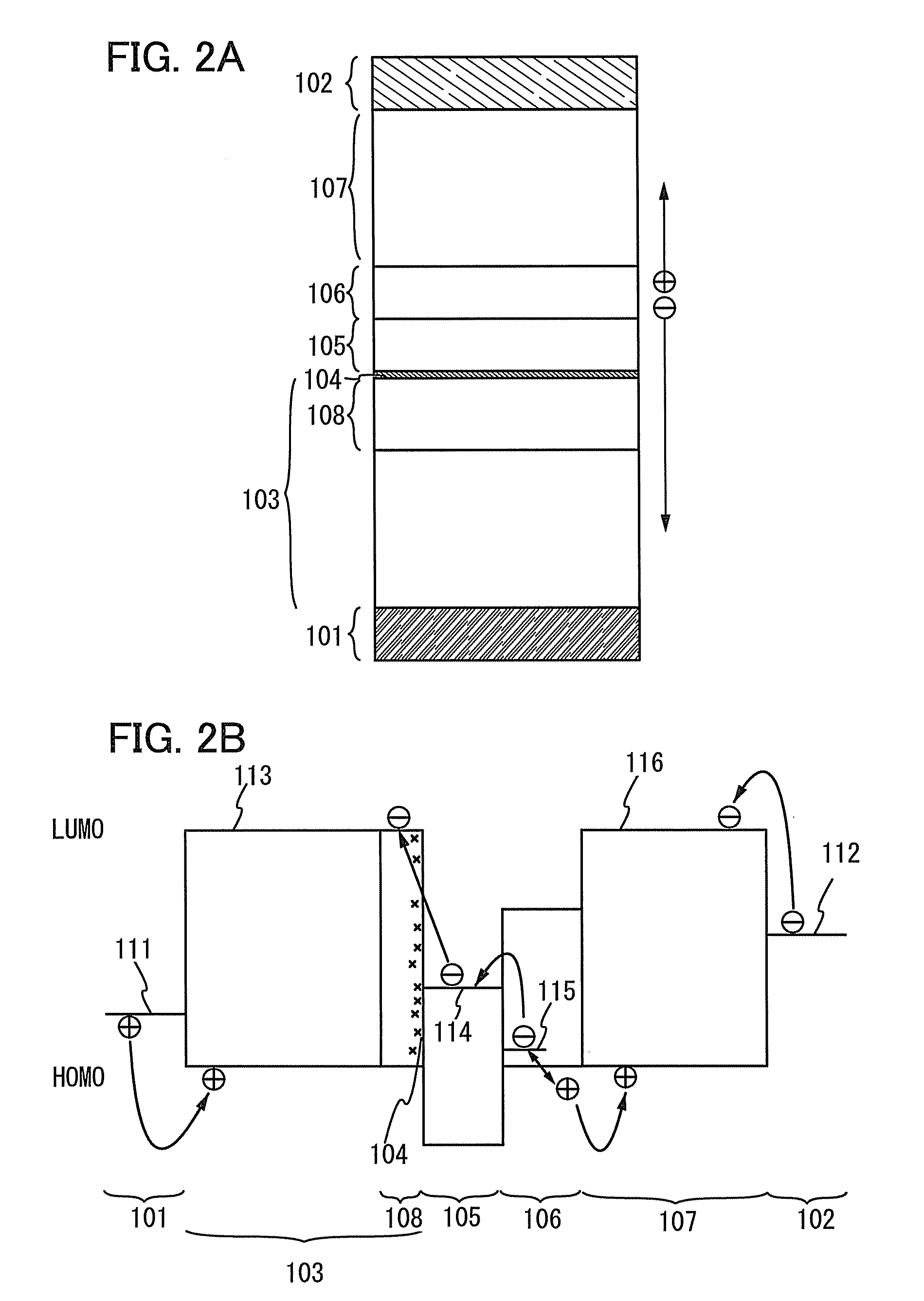
[0112]In Embodiment 3, an example of the light-emitting element included in the basic structure described in Embodiment 1 will be described with reference to FIGS. 3A and 3B. Specifically, a case where the electron-injection buffer 104 in the light-emitting element described in Embodiment 1 contains a substance having high electron-transport properties and a donor substance.

[0113]As illustrated in FIG. 3A, in a light-emitting element described in this embodiment, the first EL layer 103 and the second EL layer 107 each including a light-emitting region are interposed between a pair of electrodes (i.e., the anode 101 and the cathode 102), and between the first EL layer 103 and the second EL layer 107, the electron-injection buffer 104, the electron-relay layer 105, and the charge-generation layer 106 are stacked in this order over the anode 101. In addition, the electron-injection buffer 104 contains a substance having high electron-transport properties and a donor substance.

[0114]Not...


PUM


Abstract

A light-emitting element is provided, in which n (n is a natural number of two or more) EL layers are provided between an anode and a cathode. Between the m-th (in is a natural number, 1≦m≦n−1) EL layer and the (m+1)-th EL layer, a first layer containing any of an alkali metal, an alkaline earth metal, a rare earth metal, an alkali metal compound, an alkaline earth metal compound, and a rare earth metal compound, a second layer containing a substance having high electron-transport properties in contact with the first layer, and a charge-generation layer containing a substance having high hole-transport properties and an acceptor substance in contact with the second layer are provided in this order over the anode. The charge-generation layer does not have a peak of an absorption spectrum in a visible light region.

Description

TECHNICAL FIELD[0001]The present invention hereinafter disclosed relates to a light-emitting element including a light-emitting layer between a pair of electrodes. The present invention also relates to a light-emitting device in which the light-emitting element is used and a lighting device and an electronic device in each of which the light-emitting device is used.BACKGROUND ART[0002]In recent years, a light-emitting element in which a light-emitting organic compound or a light-emitting inorganic compound is used as a light-emitting substance has been actively developed. In particular, a light-emitting element called an electroluminescence (hereinafter, EL) element has a simple structure in which a light-emitting layer containing a light-emitting substance is provided between electrodes, and has attracted attention as a next-generation flat panel display element because of its characteristics such as thinness, lightweight, high response speed, and direct current low voltage driving...

Claims


Application Information

Patent Timeline
IPC IPC(8): H01L51/54
CPCH01L27/3209H01L51/001H01L51/5278H01L51/006H01L51/0081H01L51/0053H10K59/32H10K71/164H10K85/621H10K85/633H10K85/324H10K50/19Y10S428/917H10K85/654H10K85/00H10K50/11H10K50/13H10K50/15H10K50/16H10K50/81H10K50/82H10K2101/40
Inventor NOWATARI, HIROMISEO, SATOSHI
Owner SEMICON ENERGY LAB CO LTD
Why Eureka
Try Eureka