Semiconductor device and circuit protection method

a technology of semiconductor devices and circuit protection, applied in the direction of pulse manipulation, emergency protective arrangements for limiting excess voltage/current, pulse technique, etc., can solve the problem of inability to ensure long-term reliability of resins and bonding wires, and achieve the effect of long-term reliability

Inactive Publication Date: 2011-03-10
RENESAS ELECTRONICS CORP
View PDF2 Cites 16 Cited by
  • Summary
  • Abstract
  • Description
  • Claims
  • Application Information

AI Technical Summary

Benefits of technology

[0016]According to the present invention, a semiconductor device and a circuit protection method for preventing a con

Problems solved by technology

Therefore, in a case of being in the overcurrent state for a long time due to a short-circuit of a load, the circuit is maintained in a high temperature state of the normal recovery temperature (for example, 150° C.) or more or of a rated operation temperature range (for example, 150° C.) or more, and accordingly a

Method used


Image

  • Semiconductor device and circuit protection method
  • Semiconductor device and circuit protection method
  • Semiconductor device and circuit protection method

Examples


Embodiment Construction

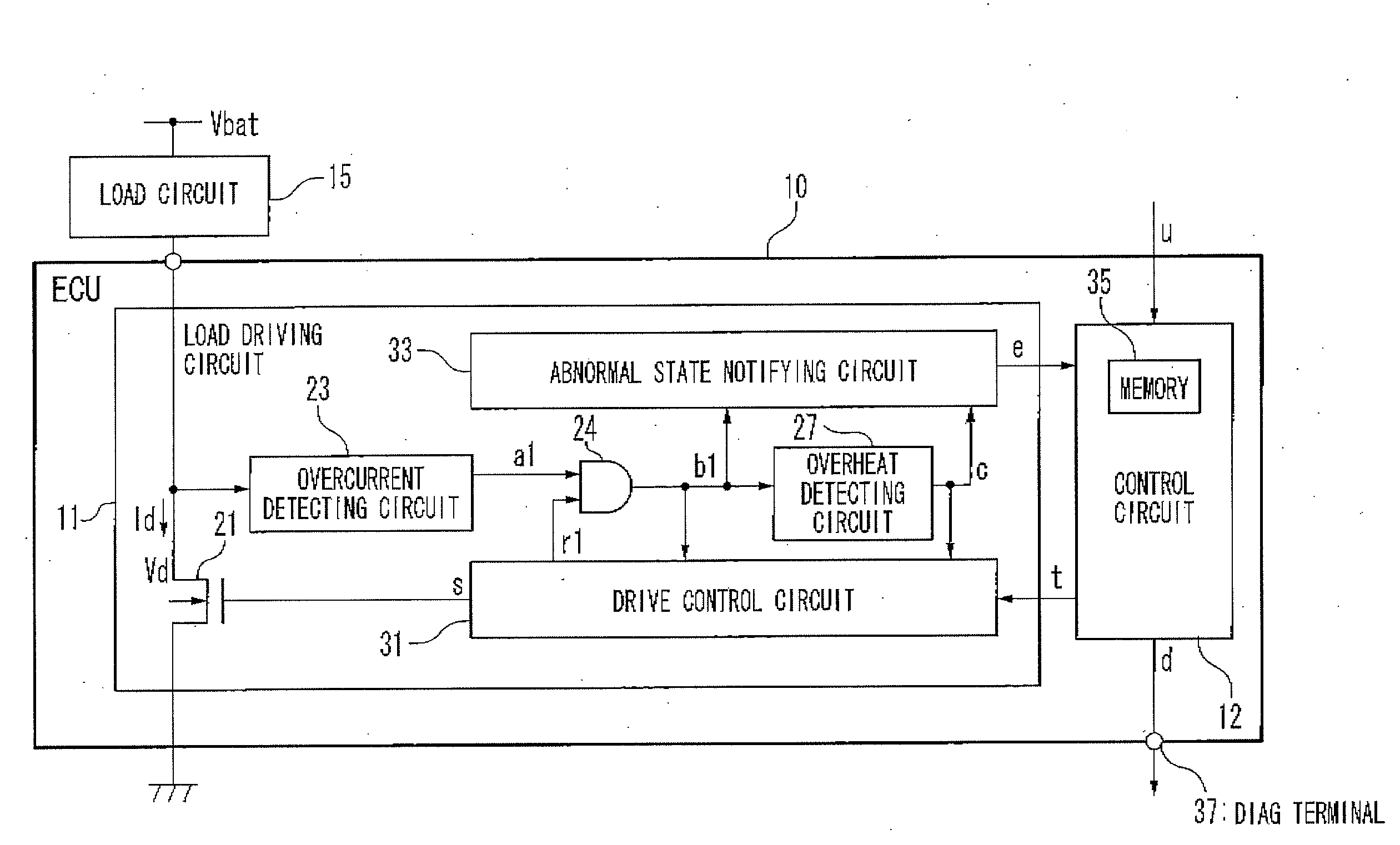
[0026]FIG. 1 shows a block diagram of a semiconductor device according to a first embodiment of the present invention. As the semiconductor device, an engine control unit (ECU) for an automobile electric component is exemplified. An engine control unit 10 includes a control circuit 12 having a memory 35, and a load driving circuit 11, and controls an electric current flowing through a load circuit 15.

[0027]The load driving circuit 11 includes an output transistor 21, an overcurrent detecting circuit 23, a detection period setting circuit 24, an overheat detecting circuit 27, a drive control circuit 31, and an abnormal state notifying circuit 33. The output transistor 21 controls a current flowing through the load circuit 15 in response to a control signal s outputted from the drive control circuit 31. A drain voltage Vd of the output transistor 21 is supplied to the overcurrent detecting circuit 23.

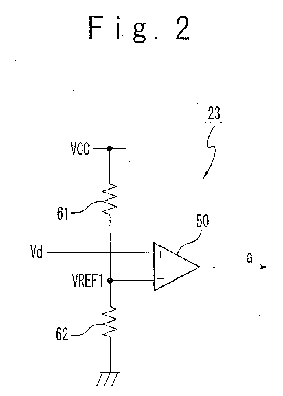
[0028]As shown in FIG. 2, the overcurrent detecting circuit 23 includes a comparator ...


PUM


Abstract

A semiconductor device includes a current supply section configured to control a current flowing through a load circuit; an overcurrent detecting section configured to detect based on the current, that an overcurrent flows through the load circuit, to output an overcurrent signal; and an overheat detecting circuit configured to detect that a peripheral temperature exceeds a detected temperature; in response to the overcurrent signal, and output an overheat detection signal. The overheat detecting circuit has a hysteresis to the detection temperature, and the detection temperature contains an overheat detection temperature used to detect an overheat state and a recovery temperature used to detect to have escaped from the overheat state. The semiconductor device further includes a drive control circuit configured to output the current control signal which indicates the quantity of the current flowing through the load circuit based on the overcurrent signal and the overheat detection signal in the electric current supply section.

Description

INCORPORATION BY REFERENCE[0001]This patent application claims a priority on convention based on Japanese Patent Application No. 2009-209105 filed on Sep. 9, 2009. The disclosure thereof is incorporated herein by reference.TECHNICAL FIELD[0002]The present invention relates to a semiconductor device, and especially relates to a semiconductor device and a circuit protecting method for detecting an overheat state to protect a circuit.BACKGROUND ART[0003]Conventionally, a relay is often used to control a large current and a high voltage. However, in an engine control unit (ECU) for automobile electric components, an IPD (Intelligent Power Device) has been increasingly used instead of the relay in these years. The IPD is provided with a circuit having a protection function around a power MOS transistor, and has a built-in self-diagnosis function. The IPD is able to transmit a self-diagnosis result to a control microprocessor.[0004]For example, as disclosed in Patent Literature 1 (JP 2000...

Claims


Application Information

Patent Timeline
IPC IPC(8): H02H9/08H03K5/125
CPCH03K17/0822H03K17/18H03K2017/0806
Inventor HIGASHIDA, YOSHIHIROTAMAGAWA, AKIO
Owner RENESAS ELECTRONICS CORP
Why Eureka
Try Eureka