Component of wireless IC device and wireless IC device

a technology of ic chip and ic device, which is applied in the direction of loop antenna, basic electric elements, instruments, etc., can solve the problems of unstable operation of wireless tag, increased size of wireless tag, and increased size of ic chip, etc., to achieve significant design freedom of feeding circuit, increase q value of inductance element, and stabilize communication characteristics

Active Publication Date: 2011-03-17
MURATA MFG CO LTD
View PDF99 Cites 14 Cited by
  • Summary
  • Abstract
  • Description
  • Claims
  • Application Information

AI Technical Summary

Benefits of technology

[0015]Preferably, the inductance element is defined by at least one annular electrode having a substantially annular shape by a via hole conductor provided in the feeding circuit substrate and the plurality of electrodes, and the winding axis of the annular electrode is perpendicular or substantially perpendicular to the lamination direction of the feeding circuit substrate. With this configuration, a magnetic field is generated on the inner side of the annular electrode and in a direction perpendicular or substantially perpendicular to the lamination direction of the feeding circuit substrate. As a result, when the feeding circuit substrate is arranged in proximity to an article using the second main surface of the feeding circuit substrate as a mounting surface, a magnetic field is generated in parallel or substantially in parallel with the mounting surface. Therefore, the electromagnetic field generated by the feeding circuit is not significantly affected by the article, and stabilized communication characteristics are obtained. Furthermore, since a via hole conductor inside the feeding circuit substrate defines a portion of the inductance element, the Q value of the inductance element is increased. Thus, a feeding circuit having satisfactory electrical characteristics is provided.
[0016]Preferably, when the annular electrode is viewed from a direction perpendicular or substantially perpendicular to the lamination direction, the wireless IC is arranged on an inner side of the annular electrode and a portion of the annular electrode is arranged in proximity to the radiation plate. With such a arrangement, the entire feeding circuit substrate can used to configure the feeding circuit, and thus, the degree of design freedom of the feeding circuit is significantly increased. Furthermore, since the feeding circuit can be arranged in proximity to the main surface to be coupled to the radiation plate, the coupling between the feeding circuit and the radiation plate can be increased, and radiation characteristics of the signal in the radiation plate can be significantly improved.
[0017]The feeding circuit may preferably include capacitance elements arranged such that the plurality of electrodes oppose one another, and the plurality of electrodes defining the capacitance elements may also define the stress alleviating electrodes. As a result of the electrodes defining the capacitance elements being arranged in a direction perpendicular or substantially perpendicular to the lamination direction of the feeding circuit substrate, the direction of the magnetic field generated in the annular electrode defining the inductance element is parallel or substantially parallel to the extension direction of the electrodes. As a result, the magnetic field generated in the inductance element is not disturbed by the electrodes defining the capacitance element, desired design values can be obtained, and a feeding circuit having predetermined resonance characteristics and matching characteristics can be obtained. Furthermore, the electrodes defining the capacitance element may define a stress alleviating electrode, the electrode being arranged directly above and / or directly below the wireless IC. With such a configuration, the number of electrode layers inside the feeding circuit substrate are decreased, and the area and height of the wireless IC device are further decreased.
[0018]Preferably, the feeding circuit substrate includes a flexible portion and a rigid portion, and the wireless IC is arranged in the rigid portion. Since the feeding circuit substrate includes a plurality of resin layers, the feeding circuit substrate is flexible. However, if the feeding circuit substrate is configured to be partially rigid and a wireless IC is arranged in the rigid portion, the stress on the wireless IC can be effectively reduced. The portion in which the annular electrode and the stress alleviating electrode are provided defines a rigid portion in which bending is prevented. In particular, if the annular electrode is formed using a copper foil, it is possible to make the inner side portion of the annular electrode rigid.
[0019]Preferably, a frequency of a signal that is transmitted and received in the radiation plate is substantially determined in accordance with a resonance frequency of the feeding circuit. As described above, by substantially determining the frequency of the signal to be used for communication based on the resonance frequency in the feeding circuit, even if the shape or the material of an article in which the radiation plate and the wireless IC device are mounted is changed, the frequency of the signal that is transmitted and received by the radiation plate is not significantly changed. For this reason, even if the wireless IC device is laminated on various articles or even if an article in which the wireless IC device is laminated is deformed, a malfunction does not occur, and the operation of the wireless IC device can be stabilized.
[0020]According to various preferred embodiments of the present invention, since a multilayered substrate includes a plurality of resin layers and a plurality of electrodes that are laminated, the area and height of the component of a wireless IC device and the wireless IC device can be decreased. Furthermore, by including the wireless IC chip in the feeding circuit substrate, the wireless IC chip can securely protected. Thus, a component of a wireless IC device and a wireless IC device having improved mechanical strength and environment resistance performance are provided.

Problems solved by technology

As described above, if the matching state between the IC chip and the main antenna element is changed, desired radiation characteristics are not obtained in the main antenna element, and a communication problem occurs with the reader / writer that performs wireless communication with the wireless tag, which presents a problem in that the operation of the wireless tag is unstable.
Furthermore, in the wireless tag, another problem is that since matching units are arranged on the sides of the IC chip on a dielectric substrate, the size of wireless tag is increased.
Furthermore, in the wireless tag, since an IC chip is arranged so as to be viewable externally on a dielectric substrate, after a wireless tag is laminated on an article, there is a possibility that the IC chip contacts another article when the article is moved or carried, which presents another problem in that the IC chip may be damaged or may detach from the dielectric substrate due to impact, and thus, the wireless tag does not operate as a wireless tag.
Furthermore, another problem is that when the IC chip is exposed to the outside, corrosion due to temperature and humidity in the periphery of the wireless tag, or other environmental factors occurs and the environmental resistance performance of the wireless tag is poor.

Method used


Image

  • Component of wireless IC device and wireless IC device
  • Component of wireless IC device and wireless IC device
  • Component of wireless IC device and wireless IC device

Examples


first preferred embodiment

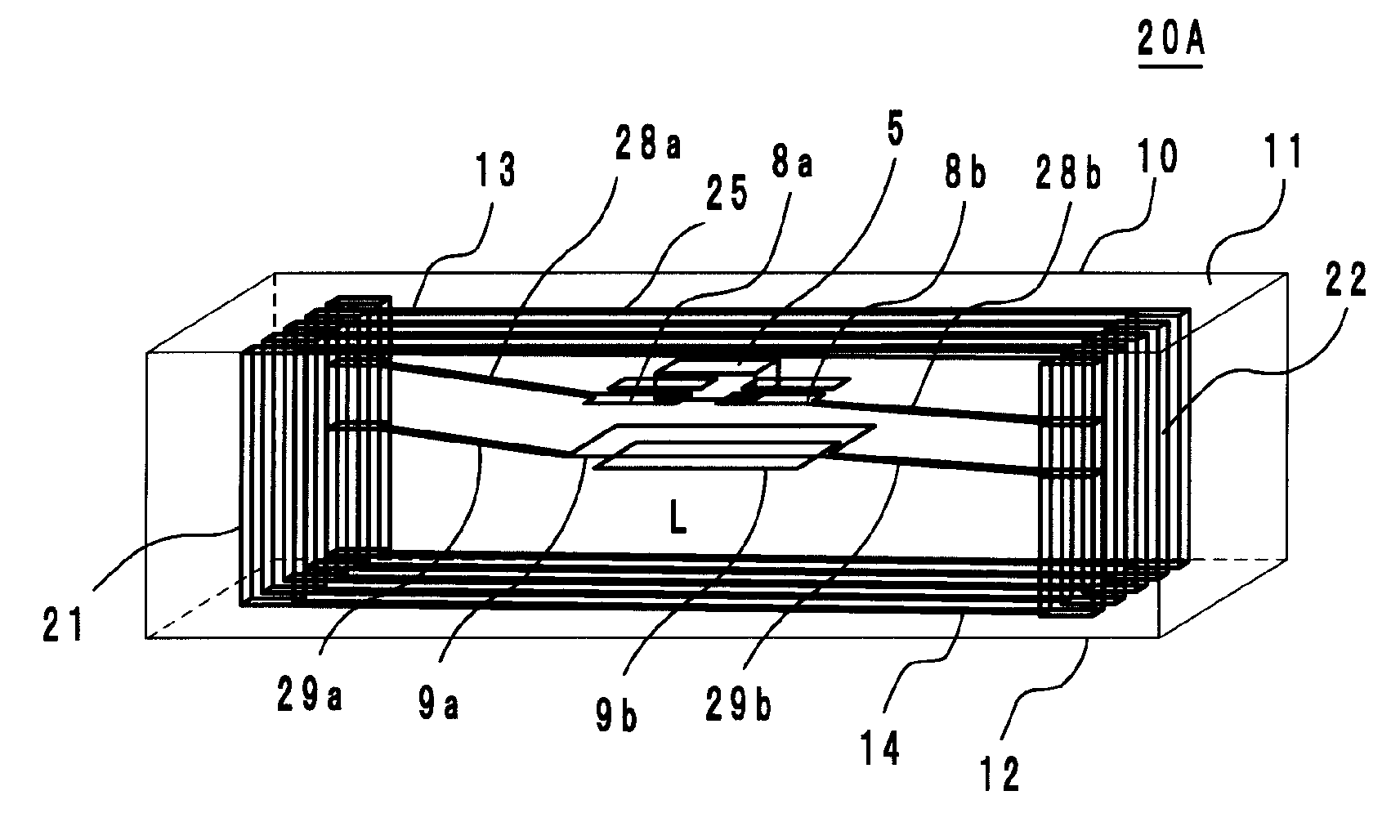
[0032]FIGS. 1 and 2 show a component 20A of a wireless IC device according to a first preferred embodiment of the present invention. FIG. 1 is a perspective view showing the internal structure of the component 20A of a wireless IC device. FIG. 2 is an exploded perspective view of each of the resin layers defining the component 20A of a wireless IC device. The component 20A of a wireless IC device is defined by a wireless IC chip 5 arranged to process a transmission / reception signal of a predetermined frequency, and a feeding circuit substrate 10 including the wireless IC chip 5 provided therein.

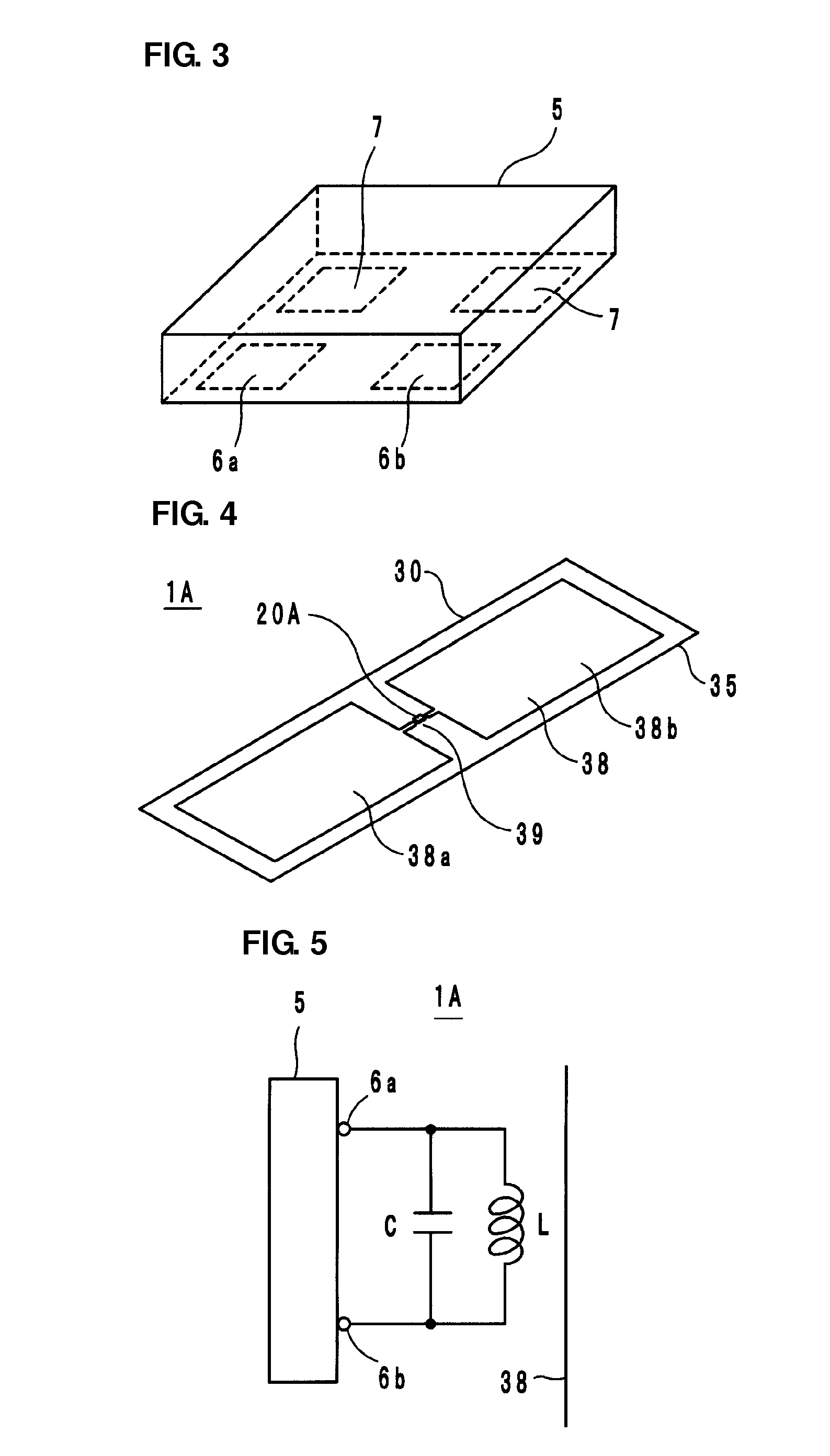
[0033]The wireless IC chip 5 preferably includes a clock circuit, a logic circuit, a memory circuit, and other suitable circuits, and includes necessary information stored therein. FIG. 3 is a perspective view showing the wireless IC chip 5 including input-output electrodes 6a and 6b and mounting terminal electrodes 7 and 7 provided on the reverse surface of the wireless IC chip 5. The input / ...

second preferred embodiment

[0048]FIG. 6 shows a component 20B of a wireless IC device according to a second preferred embodiment of the present invention. Similar to the first preferred embodiment, the component 20B is configured such that an annular electrode 55 (inductance element L) is defined by spiral electrodes 51, 52, 53, and 54 inside the feeding circuit substrate 10, and the wireless IC chip 5 is included therein.

[0049]The spiral electrodes 51 to 54 are arranged on the resin layers 61a to 61d, an end portion 51a of the spiral electrode 51 is connected to an end portion 52a of the spiral electrode 52 via a via hole conductor 62a, and an end portion 52b of the spiral electrode 52 is connected to an end portion 53a of the spiral electrode 53 via a via hole conductor 62b. Furthermore, an end portion 53b of the spiral electrode 53 is connected to an end portion 54a of the spiral electrode 54 via a via hole conductor 62c.

[0050]An end portion 51b of the spiral electrode 51 is connected to an end portion 56...

third preferred embodiment

[0053]FIG. 8 shows a component 20C of a wireless IC device according to a third preferred embodiment of the present invention. Similar to the first preferred embodiment, the component 20C is configured such that an annular electrode 77 (inductance elements L1 and L2), and opposing flat plate electrodes 83 and 84 (capacitance elements C) are defined by double linear electrodes 71, 72, 73, 74, 75, and 76 inside the feeding circuit substrate 10, and the wireless IC chip 5 is included therein.

[0054]The linear electrodes 71 to 76 are provided on resin layers 81a to 81c, an end portion 71b of the linear electrode 71 is connected to an end portion 73a of the linear electrode 73 via a via hole conductor 78a, and an end portion 73b of the linear electrode 73 is connected to an end portion 75a of the linear electrode 75 via a via hole conductor 78b. An end portion 75b of the linear electrode 75 is connected to an end portion 84a of the flat plate electrode 84 provided on the resin layer 81d v...


PUM


Abstract

A component of a wireless IC device includes a wireless IC chip and a feeding circuit substrate including a plurality of laminated resin layers. The wireless IC chip is included inside the feeding circuit substrate, and an annular electrode is arranged inside the feeding circuit substrate. The component of a wireless IC device and the radiation plate define the wireless IC device.

Description

BACKGROUND OF THE INVENTION[0001]1. Field of the Invention[0002]The present invention relates to a component of a wireless IC device including a wireless IC for use with an RFID (Radio Frequency Identification) system, and also relates to the wireless IC device.[0003]2. Description of the Related Art[0004]Recently, as an article management system, an RFID system has been developed in which communication is performed between a reader / writer that generates an induced electromagnetic field and an IC chip (also referred to as an IC tag, a wireless tag, or a wireless IC chip) with a non-contact method so that information is transferred, the IC chip including predetermined information stored therein and being provided in an article, a container, or other object. It is possible for an IC chip, as a result of being connected to an antenna, that is, a radiation plate, to communicate with a reader / writer. As a wireless tag including an IC chip provided therein, a wireless tag is disclosed in ...

Claims


Application Information

Patent Timeline
Patent Type & Authority Applications(United States)
IPC IPC(8): G06K19/077
CPCG06K19/07749H01Q7/00H01Q1/2225
Inventor KATO, NOBORUSASAKI, JUN
Owner MURATA MFG CO LTD
Why Eureka
Try Eureka