2t2r-1t1r mix mode phase change memory array

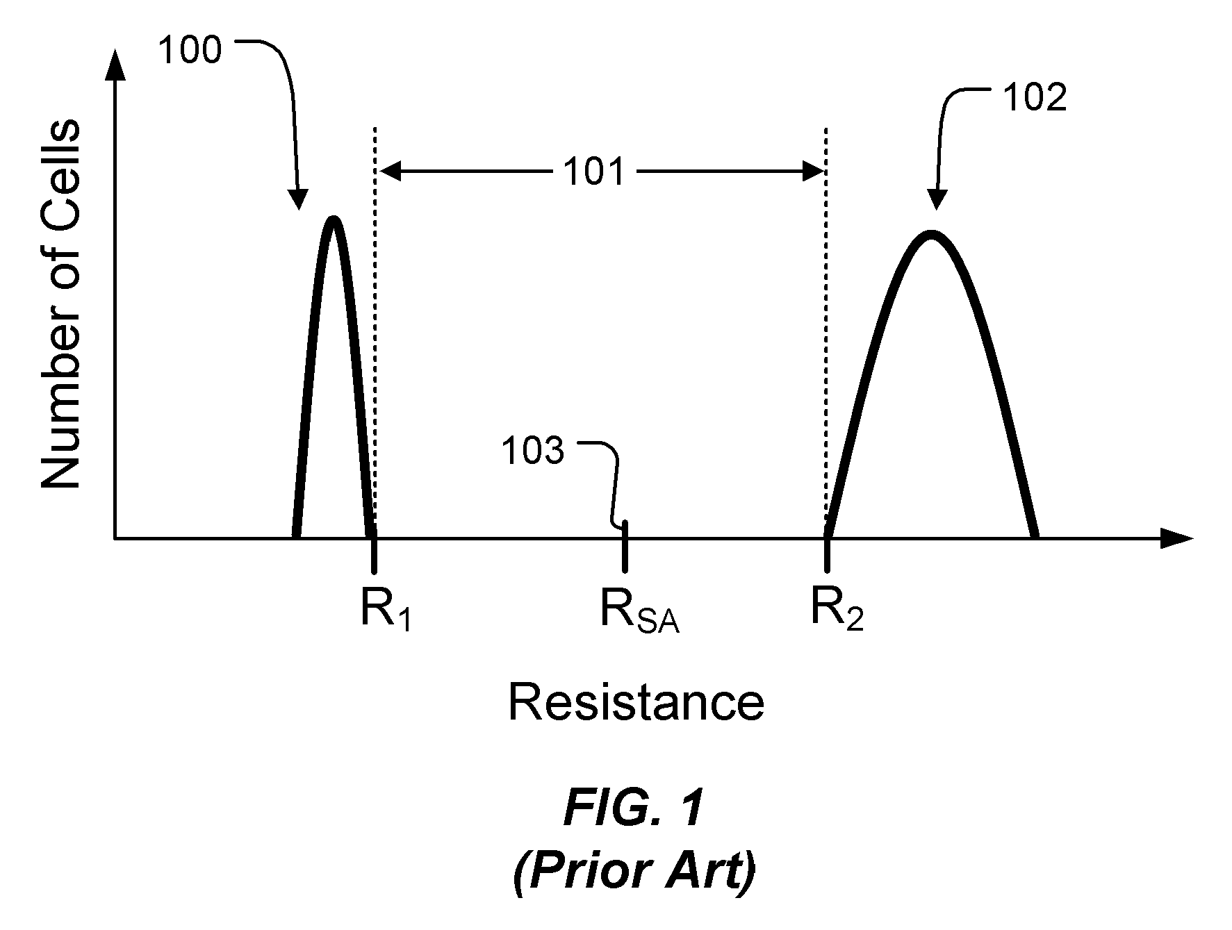
a phase change, memory array technology, applied in the field of memory devices, can solve the problems of data error, data retention problem and bit error of those memory cells, data error, similar problems can arise in other types of programmable resistance materials, etc., to achieve excellent nonvolatile data retention performance, high speed operation of memory cells, and reliable distinguishing

Active Publication Date: 2011-03-17
MACRONIX INT CO LTD
View PDF99 Cites 17 Cited by
  • Summary
  • Abstract
  • Description
  • Claims
  • Application Information

AI Technical Summary

Benefits of technology

[0016]The difference between the dual mode low and high resistance states can be smaller than the single mode read margin. As a result, the time and / or energy needed to cause a transition between the dual mode low and high resistance states to store a data value can be less than the energy needed to cause a transition between the single mode low and high resistance states to store a data value. Thus, the dual memory cell mode enables high speed operation of memory cells in the array using small programming current.
[0017]The single and dual modes can provide different operational characteristics such as switching speed, operational current, and data retention within the same memory cells of an array. As a result, the array can address the different memory performance requirements demanded by various functions of an integrated circuit. Some of the memory cells in the array may be operated in the single mode while others are concurrently operated in a dual mode.

Problems solved by technology

It has been observed that some phase change memory cells in the reset state experience a decrease in resistance over time to below a threshold value used to distinguish between the reset and set states, resulting in data retention problems and bit errors for those memory cells.
If these crystalline regions connect to form a low resistance path through the active region, when the memory cell is read a lower resistance state will be detected and result in a data error.
Similar issues can arise in other types of programmable resistance materials.
However, in phase change memory, a relatively large margin typically requires a slow set operation and high reset current in order to obtain the large difference in resistance between the set and reset states.
The relatively slow set speed and a high reset current limit the operational speed of the device, restricting the use of phase change based memory circuits as high speed memory.
However, integration of different types of memory circuits for the various memory applications can be difficult and result in highly complex designs.

Method used


Image

  • 2t2r-1t1r mix mode phase change memory array
  • 2t2r-1t1r mix mode phase change memory array
  • 2t2r-1t1r mix mode phase change memory array

Examples


first embodiment

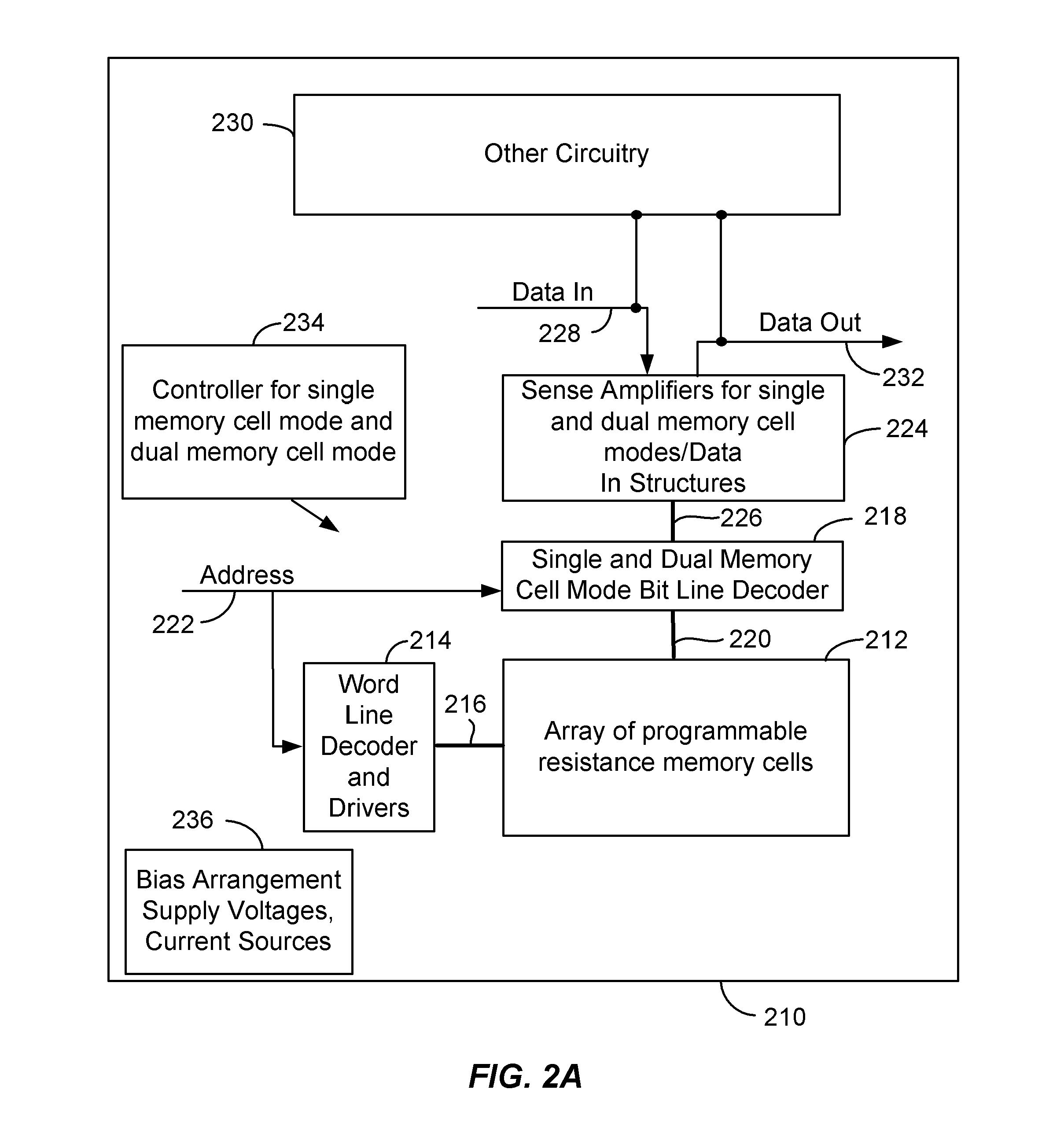
[0032]FIG. 2A is a block diagram of an integrated circuit 210 including a memory array 212 of programmable resistance memory cells. The memory cells include an access device such as a diode or transistor, and a programmable resistance memory element. As described in more detail below, the integrated circuit 210 is operable in a dual (2T-2R) mode to store a data value in a pair of memory cells in the array 212 based on a difference in resistance of a first memory cell in the pair and a second memory cell in the pair to provide high speed operation of memory cells in the array. The memory device is operable in a single (1T-1R) mode to store a data value in a particular memory cell in the array 212 based on the resistance of the particular memory cell to provide excellent nonvolatile data retention performance and higher memory density.

[0033]A word line decoder 214 is coupled to and in electrical communication with a plurality of word lines 216 arranged along rows in the memory array 2...

second embodiment

[0037]FIG. 2B is a block diagram of an integrated circuit 310 operable in the single and dual modes. The integrated circuit 310 of FIG. 2B includes a single mode sense amplifiers of block 224-1 coupled to a single mode bit line decoder 218-1 via data bus 226-1. The single mode bit line decoder 218-1 is coupled to a first memory array 212-1 via bit lines 220-1, and word line decoder and drivers 214-1 is coupled to the first memory array 212-1 via word lines 216-1, so that the memory cells of the array 212-1 operate in the single mode. Dual mode sense amplifiers of block 224-2 is coupled to dual mode bit line decoder 218-2 via data bus 226-2. A second memory array 212-1 separate from the first memory array 212-1 is coupled to a dual mode bit line decoder 218-2 via bit lines 220-2, and coupled to word line decoder and drivers 214-2 via word lines 216-2, so that the cells in the second memory array 212-2 operate in the dual mode.

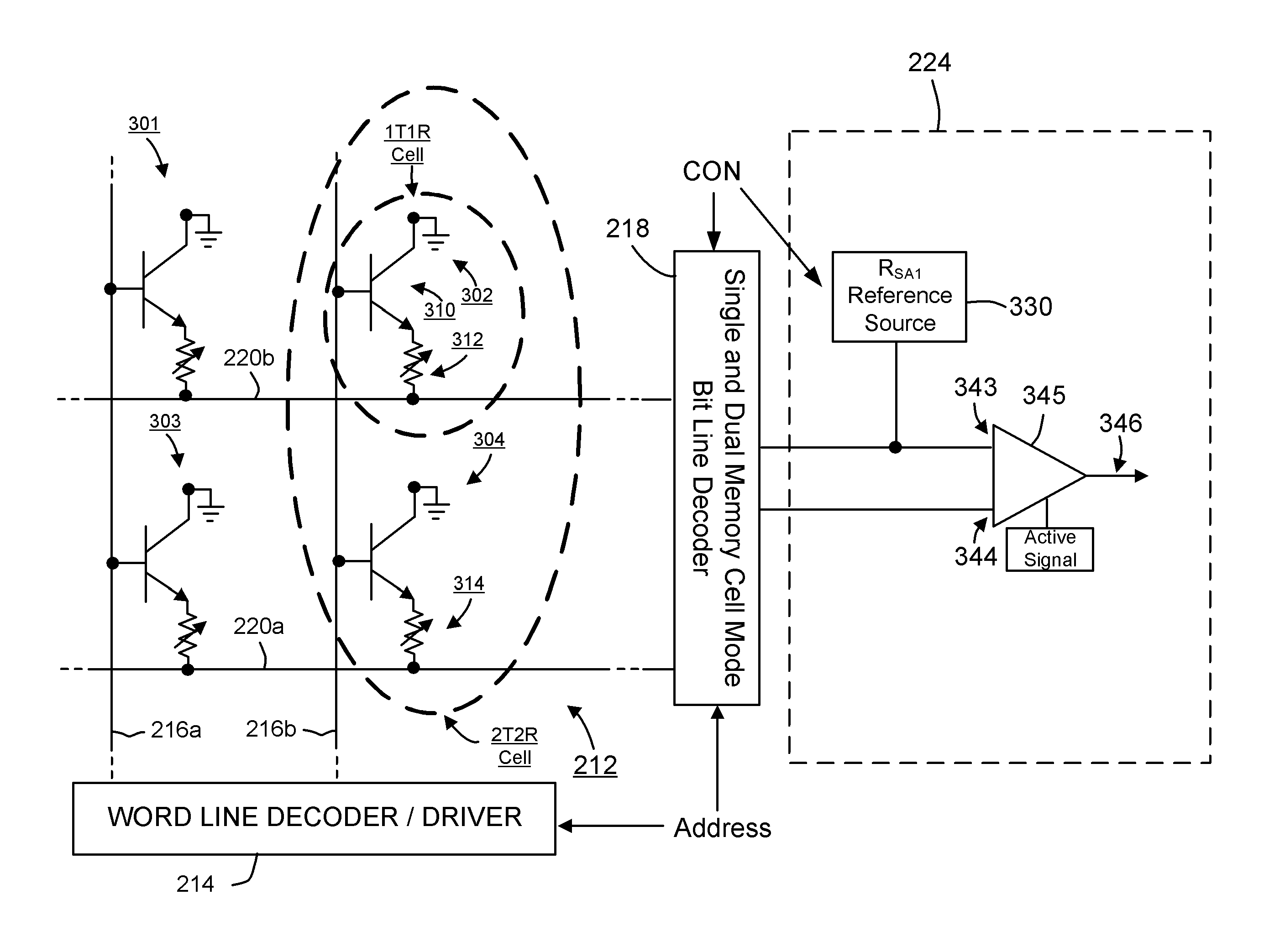
[0038]FIG. 3A illustrates a schematic diagram of an embodi...


PUM


Abstract

A memory device as described herein includes an array of programmable resistance memory cells. The memory device further includes sense circuitry having a dual memory cell (2T-2R) mode to read a data value stored in a pair of memory cells in the array based on a difference in resistance between a first memory cell in the pair and a second memory cell in the pair. The sense circuitry also has a single memory cell (1T-1R) mode to read a data value in a particular memory cell in the array based on the resistance of the particular memory cell.

Description

PARTIES TO A JOINT RESEARCH AGREEMENT[0001]International Business Machines Corporation, a New York corporation, and Macronix International Corporation, Ltd, a Taiwan corporation, are parties to a Joint Research Agreement.BACKGROUND OF THE INVENTION[0002]1. Field of the Invention[0003]The present invention relates to memory devices based on programmable resistance materials memory materials, including chalcogenide based materials and other phase change materials, and methods for operating such devices.[0004]2. Description of Related Art[0005]In general, system-on-a-chip (SOC) technology is the integration of multiple subsystems of an electronic system within a single integrated circuit, and may contain digital, analog, mixed-signal, and radio-frequency functions. The various types of subsystems that may be integrated within the integrated circuit include microprocessor and microcontroller cores, digital signal processors (DSPs), configurable logic units, memory blocks, timing sources...

Claims


Application Information

Patent Timeline
Patent Type & Authority Applications(United States)
IPC IPC(8): G11C11/00G11C7/00
CPCG11C7/067G11C7/1045G11C13/0004G11C2013/0054G11C13/004G11C2013/0042G11C13/0026
Inventor LUNG, HSIANG-LAN
Owner MACRONIX INT CO LTD
Why Eureka
Try Eureka