Gallium nitride substrate

a technology of gallium nitride and substrate, which is applied in the direction of crystal growth process, polycrystalline material growth, after-treatment details, etc., can solve the problems of substrate stress, increase in dislocation density, warpage of devices, etc., and achieves the effect of less likely to break and hard to crack

Active Publication Date: 2011-03-31
SUMITOMO ELECTRIC IND LTD
View PDF13 Cites 5 Cited by
  • Summary
  • Abstract
  • Description
  • Claims
  • Application Information

AI Technical Summary

Benefits of technology

[0018]As described above, an aspect of the present invention provides the GaN substrate hard to crack and less likely to break.

Problems solved by technology

However, the GaN-based compound semiconductor grown on the heterogeneous substrate causes problems such as stress in the substrate because of lattice mismatch, and a difference between the coefficients of thermal expansion.
This stress brings about warpage of a device, detachment of thin film, and increase in dislocation density and, thereby, adversely affects on device characteristics.
On the other hand, a manufacturing cost per GaN substrate is high because of low growth rate of GaN crystal, raw material cost, and so forth.
Since a diameter of indium atoms is larger than that of gallium atoms, an increase in composition ratio of indium leads to an increase in internal strain in an indium-containing layer because of lattice mismatch.
As a consequence, a large piezoelectric field is produced in the indium-containing layer to lower a recombination probability, resulting in low luminous efficiency.

Method used


Image

  • Gallium nitride substrate
  • Gallium nitride substrate
  • Gallium nitride substrate

Examples


example 1

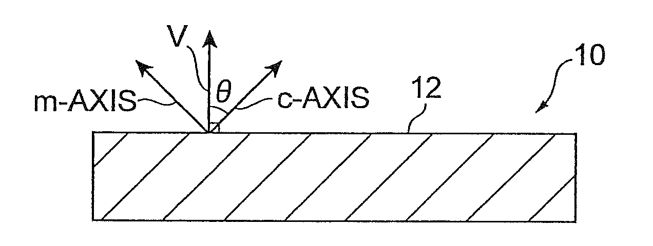
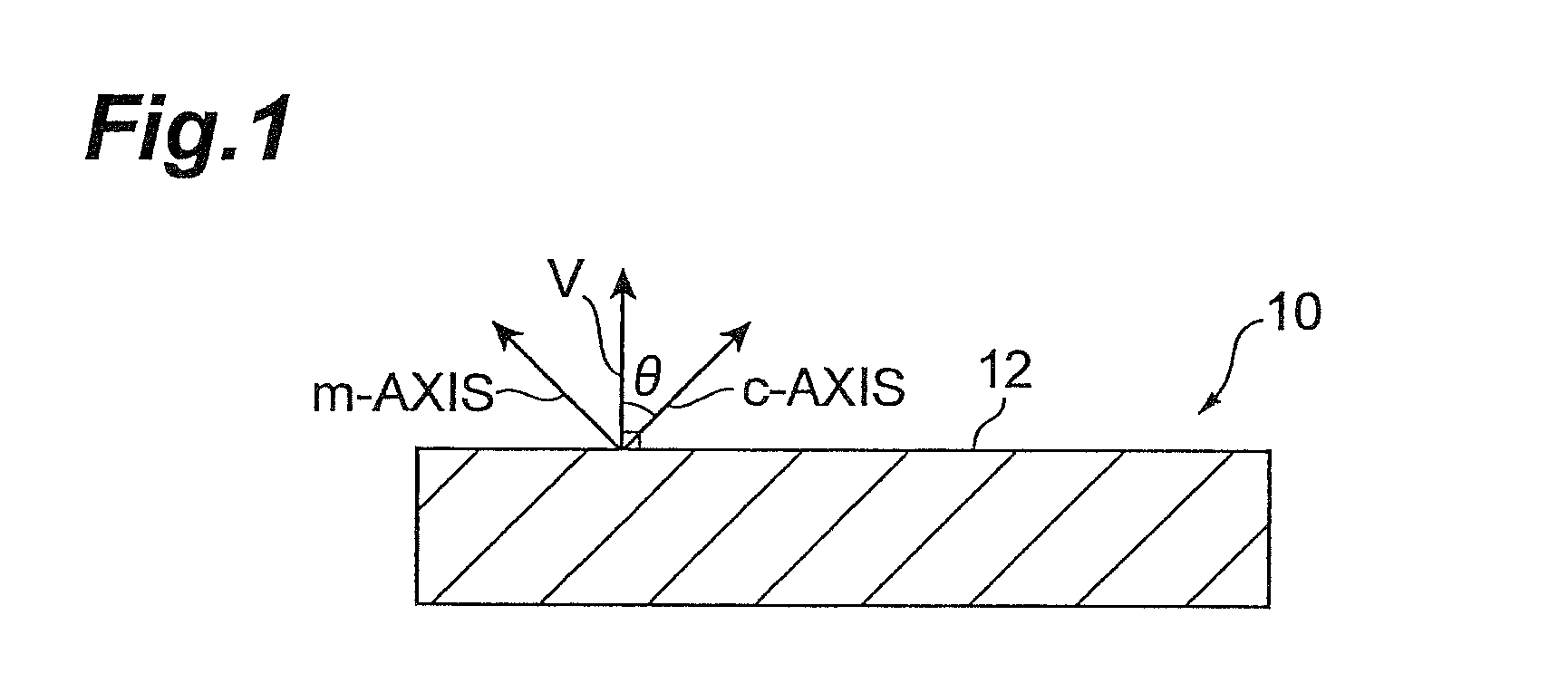
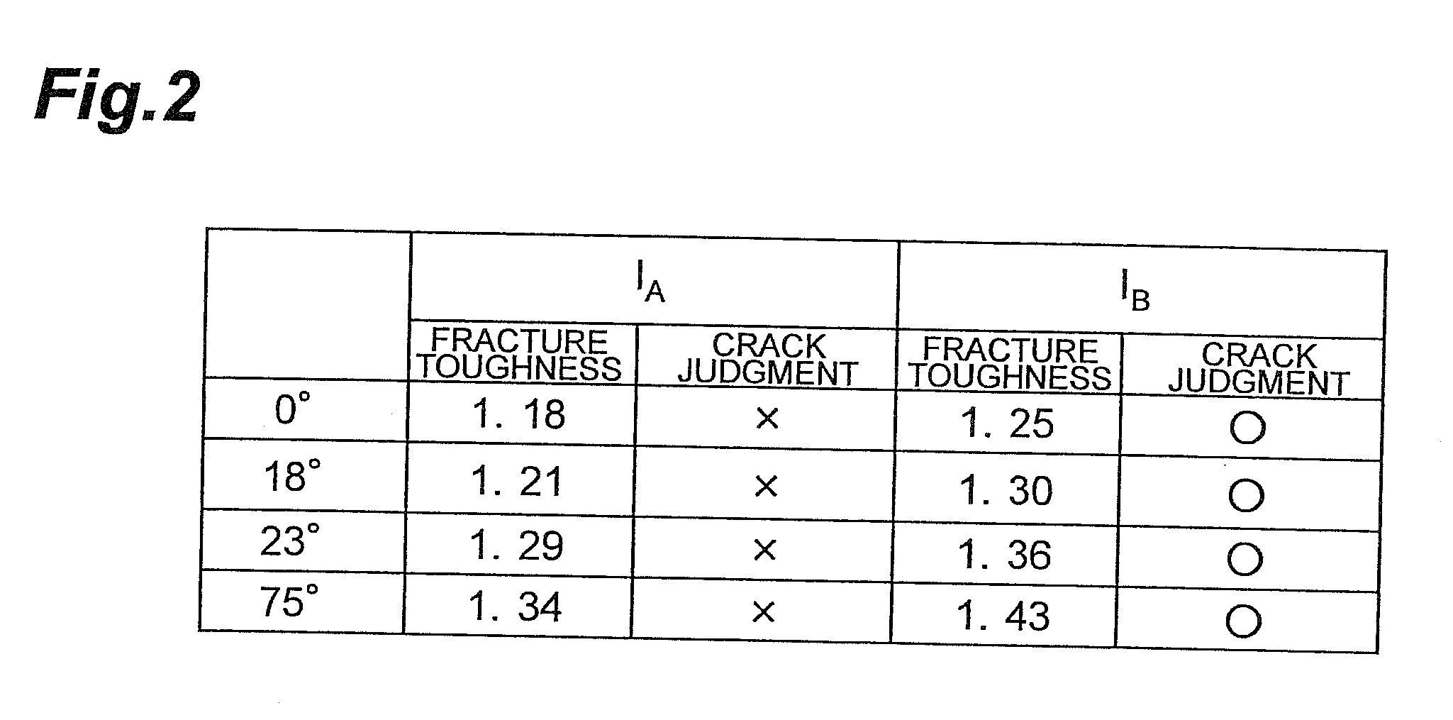
[0030]GaN ingots doped with oxygen were prepared. The GaN ingots had the diameter of two inches and the thickness of one centimeter. The GaN ingots had a primary surface that extends to the (0001) face (or C-plane) in the hexagonal structure. The GaN ingots had the electric resistivity of less than or equal to 1 Ω·cm. A carrier concentration of the GaN ingots was less than or equal to 1×1017 cm−3. In this Example, two GaN ingots IA and IB were prepared. The dopant concentration of GaN ingots IA and IB were different from each other, so that the fracture toughness values of GaN ingots IA and IB were different from each other.

[0031]These GaN ingots IA and IB were sliced to obtain eleven substrates having the thickness of 500 μm. In the slice step, the GaN ingots IA and IB were sliced at tilt angles of 0, 18, 23, and 75 degrees with respect to the [1-100] direction (or the m-axis direction) to produce four types of substrates which have respective tilt angles. The fracture toughness va...

example 2

[0033]The GaN ingot IB used in Example 1 was prepared. Two types of substrates WA and WB with the cut surface having their respective tilt angles of 23 and 75 degrees were prepared, ten for each type, by slicing the GaN ingot IB from the [11-20] direction (or the a-axis direction) and tilting the cut surface in the [11-20] direction with respect to the C-plane. Furthermore, two types of substrates WC and WD with the cut surface having their respective tilt angles of 23 and 75 degrees were prepared, ten for each type, by slicing the GaN ingot IB from the [1-100] direction and tilting the cut surface in the [1-100] direction with respect to the C-plane. These substrates WA-WD had the thickness of 500 μm after sliced, and they were then ground and polished to the thickness of 400 μm.

[0034]FIG. 3 is a graph showing the numbers of substrates remaining unbroken after the processing, out of ten of each type of the substrates WA-WD. As shown in FIG. 3, when the substrates WA and WB that hav...

example 3

[0035]A load was applied to the substrate WB with the primary surface tilted 75 degrees in the [1-100] direction, which was produced in Example 2 above. This test was carried out with a dynamic micro hardness tester (DUH-201S available from Shimadzu Corporation). The load was applied in such a manner that projected directions on the surface of the substrate WB of ridge lines of a triangular pyramid Berkovich indenter (in other words, extending directions of depressed lines of indentations in the surface when viewed from the direction normal to the surface of the substrate WB) coincided with the [11-20] direction (a-axis direction) and a direction perpendicular to the [11-20] direction. On this occasion, the load was 100 gF (1 gF is equivalent to 9.80665 g·m / s2) and the loading time was two seconds.

[0036]In this Example, the application of the load caused the substrate WB to crack, the crack extended in the direction perpendicular to the [11-20] direction independent of the orientati...


PUM

PropertyMeasurementUnit
angleaaaaaaaaaa
areaaaaaaaaaaa
angleaaaaaaaaaa

Abstract

A gallium nitride substrate comprising a primary surface, the primary surface being tilted at an angle in a range of 20 to 160 degrees with respect to a C-plane of the substrate, and the substrate having a fracture toughness of more than or equal to 1.36 MN/m3/2.

Description

BACKGROUND OF THE INVENTION[0001]1. Field of the Invention[0002]The present invention relates to a gallium nitride (GaN) substrate.[0003]2. Related Background Art[0004]A substrate composed of single crystal nitride semiconductor is disclosed (cf. Japanese Unexamined Patent Application Publication No. 2006-044982). This substrate includes AlXGa1-XN (0≦X≦1) in composition and has a fracture toughness value of more than or equal to (1.2−0.7×) MPa·m1 / 2. A primary surface of the substrate has an area of more than or equal to 20 cm2.SUMMARY OF THE INVENTION[0005]GaN-based compound semiconductors such as GaN and InGaN have a wide band gap energy. Therefore, the GaN-based compound semiconductors are expected to be applied to light emitting devices emitting short wavelength light such as blue and green light. In general, a GaN-based compound semiconductor is grown on a heterogeneous substrate made of a material (e.g., Si, SiC, or sapphire) with a coefficient of thermal expansion close to tha...

Claims


Application Information

Patent Timeline
Patent Type & Authority Applications(United States)
IPC IPC(8): H01L29/04H01L29/20
CPCC30B33/00C30B29/406
Inventor HACHIGO, AKIHIRO
Owner SUMITOMO ELECTRIC IND LTD
Why Eureka
Try Eureka