Solid-state imaging device and method for manufacturing solid-state imaging device, and electronic device

a solid-state imaging and imaging device technology, applied in the direction of solid-state devices, transistors, radiation controlled devices, etc., can solve the problems of pixel sensitivity difference, deterioration of symmetry properties of pixels, and fluctuation of well potential, so as to reduce the number of total manufacturing steps, improve pixel characteristics, and improve the effect of solid-state imaging devices

Active Publication Date: 2011-03-31
SONY CORP
View PDF6 Cites 105 Cited by
  • Summary
  • Abstract
  • Description
  • Claims
  • Application Information

AI Technical Summary

Benefits of technology

[0038]According to the solid-state imaging device of the embodiment, at least the pixel characteristic can be improved while stabilizing well potential in an effective pixel region.
[0039]According to the method for manufacturing a solid-state imaging device of the embodiment, a solid-state imaging device in which at least the pixel characteristic can be improved while stabilizing well potential in an effective pixel region can be manufactured. When the first-conductivity-type well contact region is simultaneously formed with the first conductive source / drain regions of a CMOS transistor in the peripheral circuit portion, the process of the ion implantation is cut off, being able to reduce the number of the total manufacturing steps.
[0040]The electronic device according to the embodiment of the present invention is provided with the solid-state imaging device of the embodiment described earlier, so that the pixel characteristic in the solid-state imaging device is improved. Therefore, a high quality electronic device having high image quality can be provided.

Problems solved by technology

However, in the CMOS solid-state imaging device, as the number of pixels is increased and an area of the pixel region is enlarged, such problem arises that well potential fluctuates in a semiconductor well region.
However, this case has a problem of a position at which the well contact portion is arranged and a problem of a process increase for ion implantation performed for reducing contact resistance.
Depending on the position at which the well contact portion is arranged, a symmetric property of a pixel is deteriorated, and the pixel characteristic is adversely affected by sensitivity difference among pixels.
For example, a photodiode is adversely affected depending on an impurity concentration of the well contact portion.
Further, when the well contact portion is arranged at a region close to the photodiode, there is high possibility that the well contact region adversely affects the photodiode and deteriorates the pixel characteristic.

Method used


Image

  • Solid-state imaging device and method for manufacturing solid-state imaging device, and electronic device
  • Solid-state imaging device and method for manufacturing solid-state imaging device, and electronic device
  • Solid-state imaging device and method for manufacturing solid-state imaging device, and electronic device

Examples


embodiment

2. Embodiment

[Configuration Example of Solid-State Imaging Device]

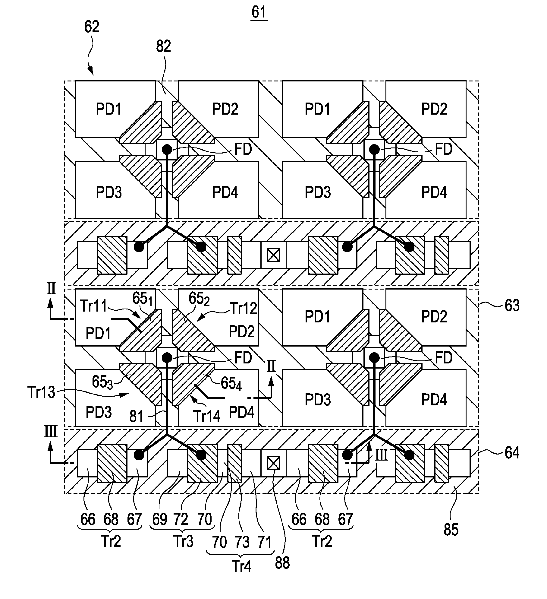
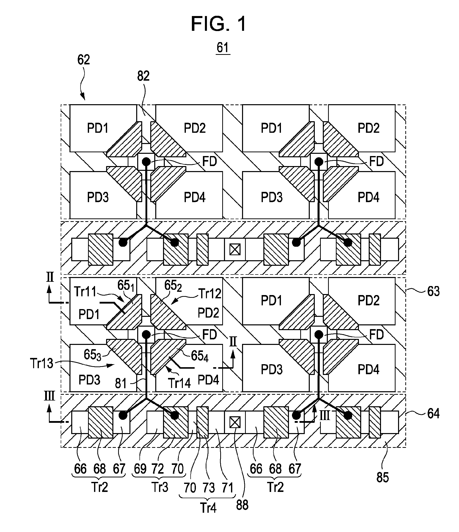
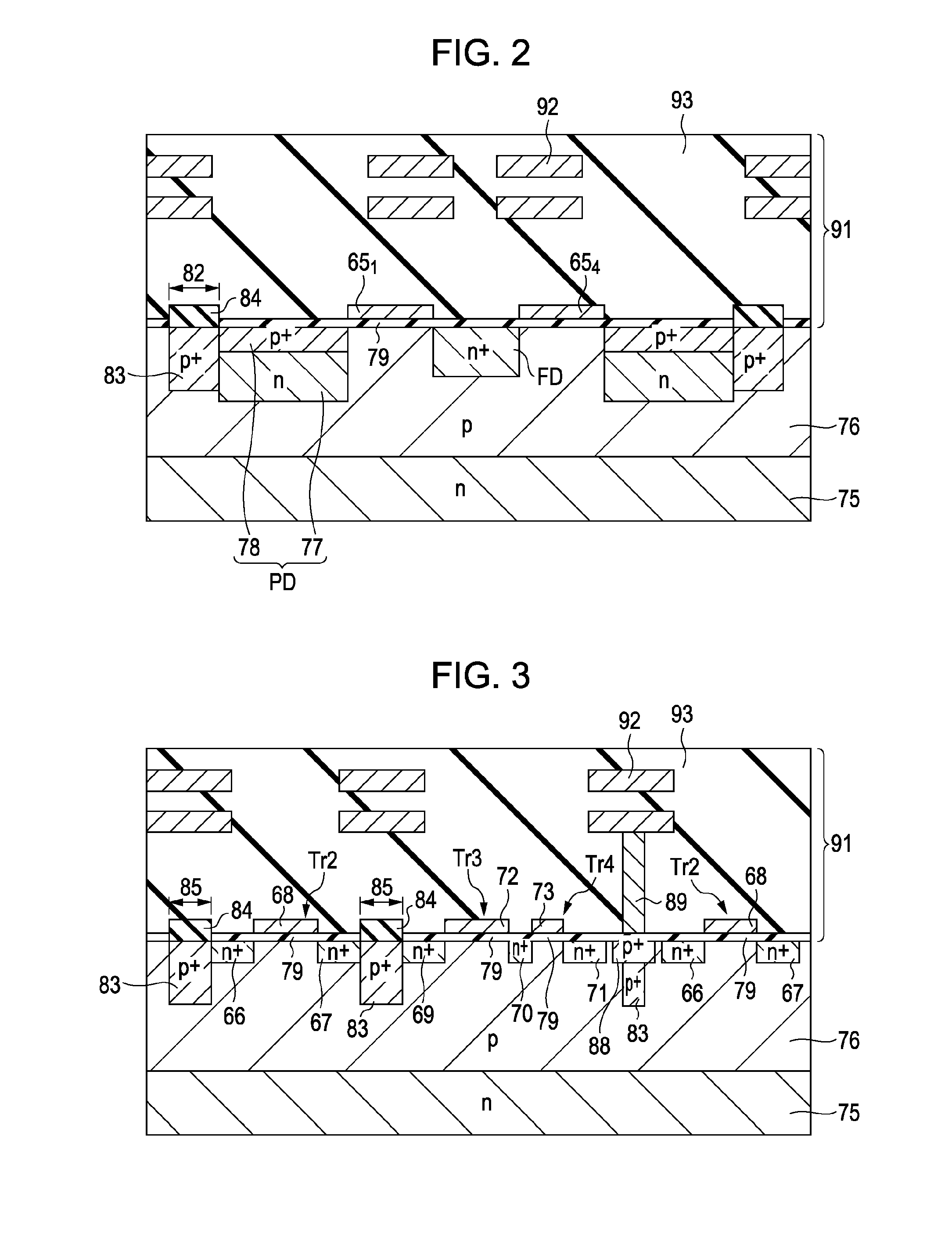
[0077]FIGS. 1 to 3 illustrate the schematic configuration of a solid-state imaging device according to an embodiment of the present invention. The solid-state imaging device of the embodiment is a CMOS solid-state imaging device and is applied to a four-pixel sharing solid-state imaging device. FIG. 1 is a plan view schematically showing a chief part of a pixel region. FIG. 2 is a sectional view taken along a II-II line of FIG. 1. FIG. 3 is a sectional view taken along a III-III line of FIG. 1.

[0078]A solid-state imaging device 61 according to the embodiment includes a pixel region 62 in which single sharing units are arranged in a two-dimensional array fashion. Each of the single sharing units is composed of photodiodes PD [PD1 to PD4] of four pixels arranged two pixels in width and two pixels in length (that is, four-pixel sharing). In a single sharing unit, one floating diffusion portion FD is shared by the four ph...


PUM


Abstract

A solid-state imaging device includes a first-conductivity-type semiconductor well region, a plurality of pixels each of which is formed on the semiconductor well region and is composed of a photoelectric conversion portion and a pixel transistor, an element isolation region provided between the pixels and in the pixels, and an element isolation region being free from an insulation film and being provided between desired pixel transistors.

Description

BACKGROUND OF THE INVENTION[0001]1. Field of the Invention[0002]The present invention relates to a solid-state imaging device and a method for manufacturing the solid-state imaging device, and an electronic device such as a camera which is equipped with the solid-state imaging device.[0003]2. Description of the Related Art[0004]As a solid-state imaging device, a CMOS solid-state imaging device is used. The CMOS solid-state imaging device has a low power-source voltage and consumes less power so as to be used in a digital still camera, a digital video camera, various mobile terminal devices such as a camera-equipped mobile phone, and the like.[0005]The CMOS solid-state imaging device includes a pixel region in which a plurality of pixels are two-dimensionally arranged in a regular manner and a peripheral circuit portion which is disposed around the pixel region. Each of the pixels is composed of a photodiode which is a photoelectric conversion portion and a plurality of pixel transis...

Claims


Application Information

Patent Timeline
Patent Type & Authority Applications(United States)
IPC IPC(8): H01L27/146H01L31/18
CPCH01L27/14603H01L27/14609H01L27/1463H01L27/14641H01L27/14643H01L27/14607H01L27/14612H01L27/14689H01L27/14636
Inventor TATANI, KEIJIKOGA, FUMIHIKONAGANO, TAKASHI
Owner SONY CORP
Why Eureka
Try Eureka