

Manufacturing method of semiconductor device and substrate processing apparatus
- Summary
- Abstract
- Description
- Claims
- Application Information
AI Technical Summary
Benefits of technology
Problems solved by technology
Method used
Image

Examples
Embodiment Construction
An Embodiment of the Present Invention
[0040]An embodiment of the present invention will be described hereafter, with reference to the drawings.
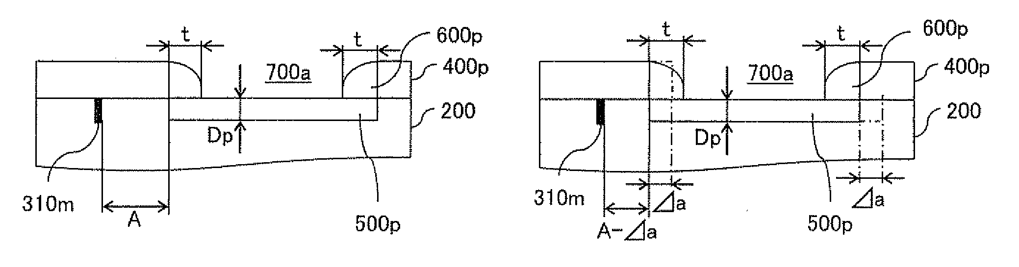
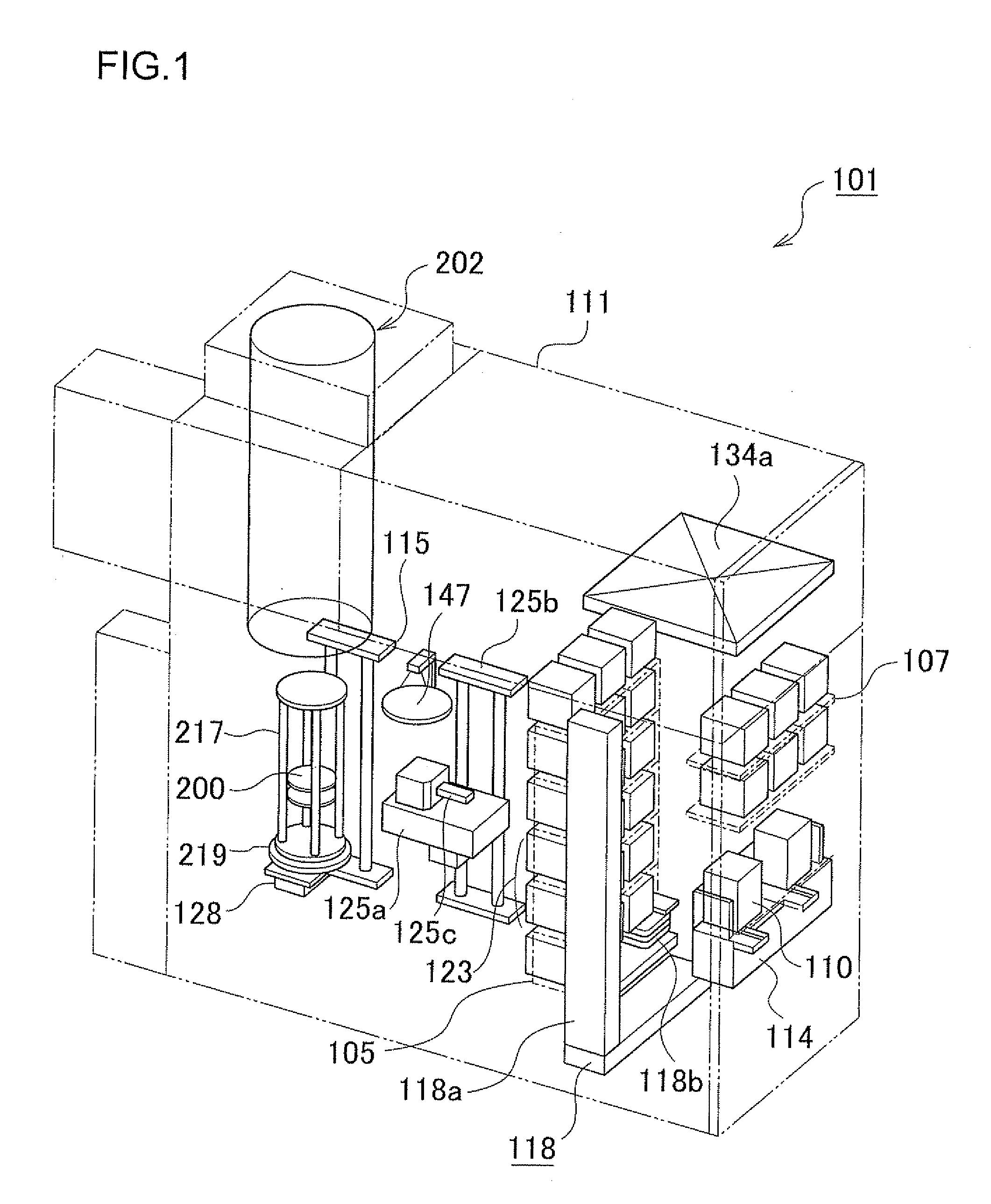
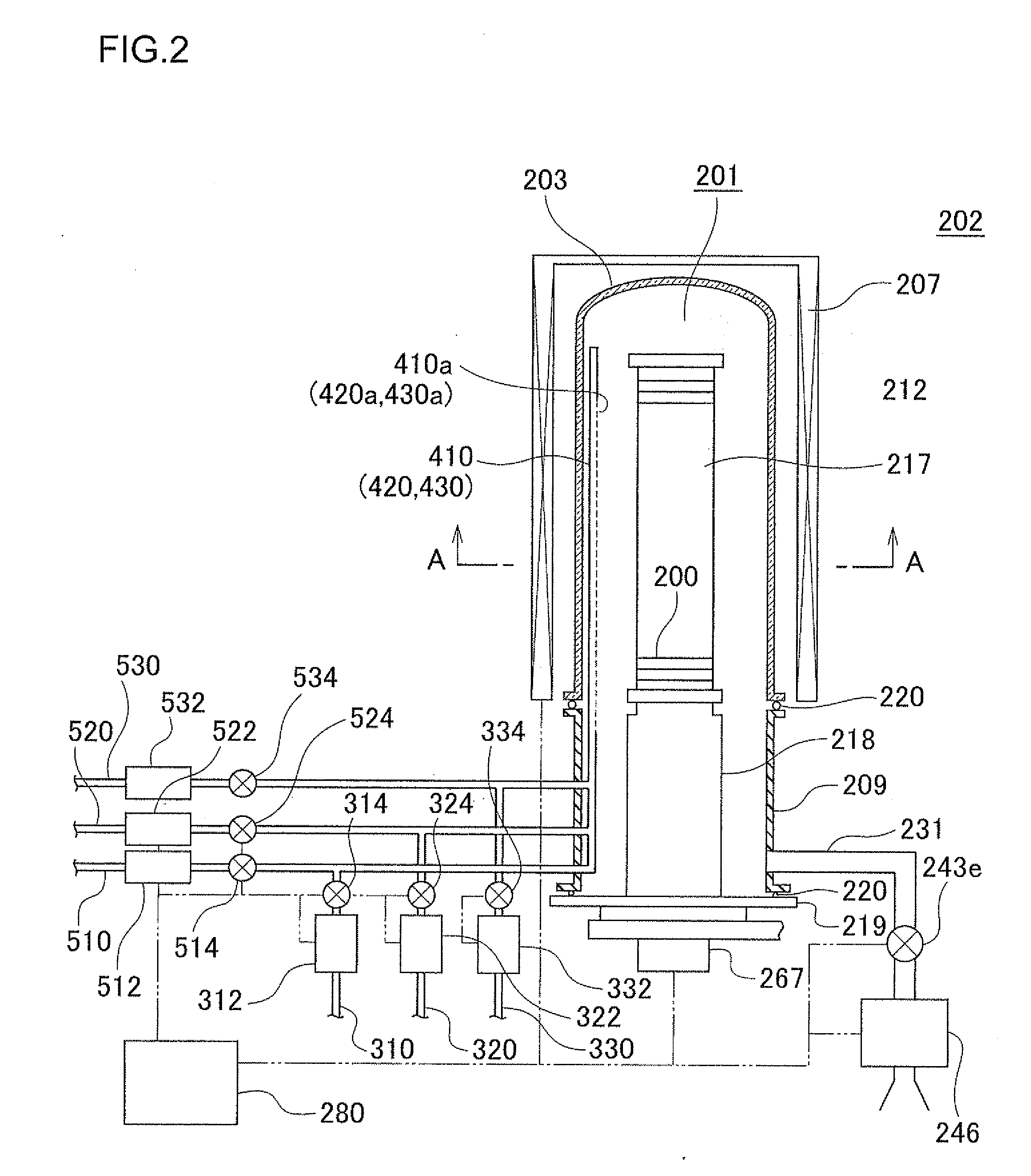
[0041]A substrate processing apparatus according to this embodiment is constituted as an example of a semiconductor manufacturing device used in manufacture of a memory device such as flush memory, DRAM (Dynamic Random Access Memory), SRAM (Static Random Access Memory) and a semiconductor device such as a logic device. In the explanation given hereafter, as an example of the substrate processing apparatus, a vertical apparatus for applying film formation processing to substrates will be described. However, the present invention is not limited to application to the vertical apparatus, and can be applied to, for example, a single wafer processor. Further, the present invention is not limited to a film formation processing of a SiO2 film (silicon oxide film) shown below, in which the Si contained source, oxide source, and catalyst are combined, ...
PUM
 Abstract
Description
Claims
Application Information