

Method of Manufacturing Selective Emitter Solar Cell
- Summary
- Abstract
- Description
- Claims
- Application Information
AI Technical Summary
Benefits of technology
Problems solved by technology
Method used
Image

Examples
Embodiment Construction
[0026]The following descriptions of the preferred embodiments are provided for understanding the features and the structures of the present disclosure.
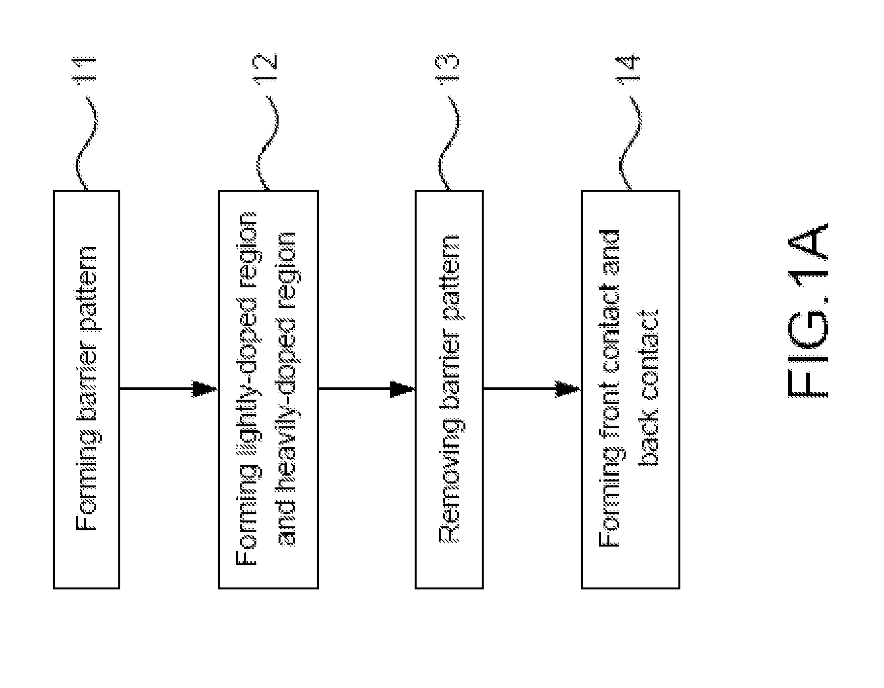
[0027]Please refer to FIG. 1A to FIG. 1F and FIG. 2 to FIG. 5, which are views showing a flow and states of use of a first preferred embodiment according to the present disclosure; a view showing a relationship among processing power, processing time, and thickness of a grown silicon nitride layer; a view showing refractive index of a grown silicon nitride layer; a view showing a relationship among processing power, processing time, and sheet resistance of a doped region; and a view showing a SIMS analysis of distribution of phosphorus atoms. As shown in these figures, the present disclosure is a method of manufacturing a selective emitter solar cell. In FIG. 1A, a first preferred embodiment according to the present disclosure comprises the following steps:
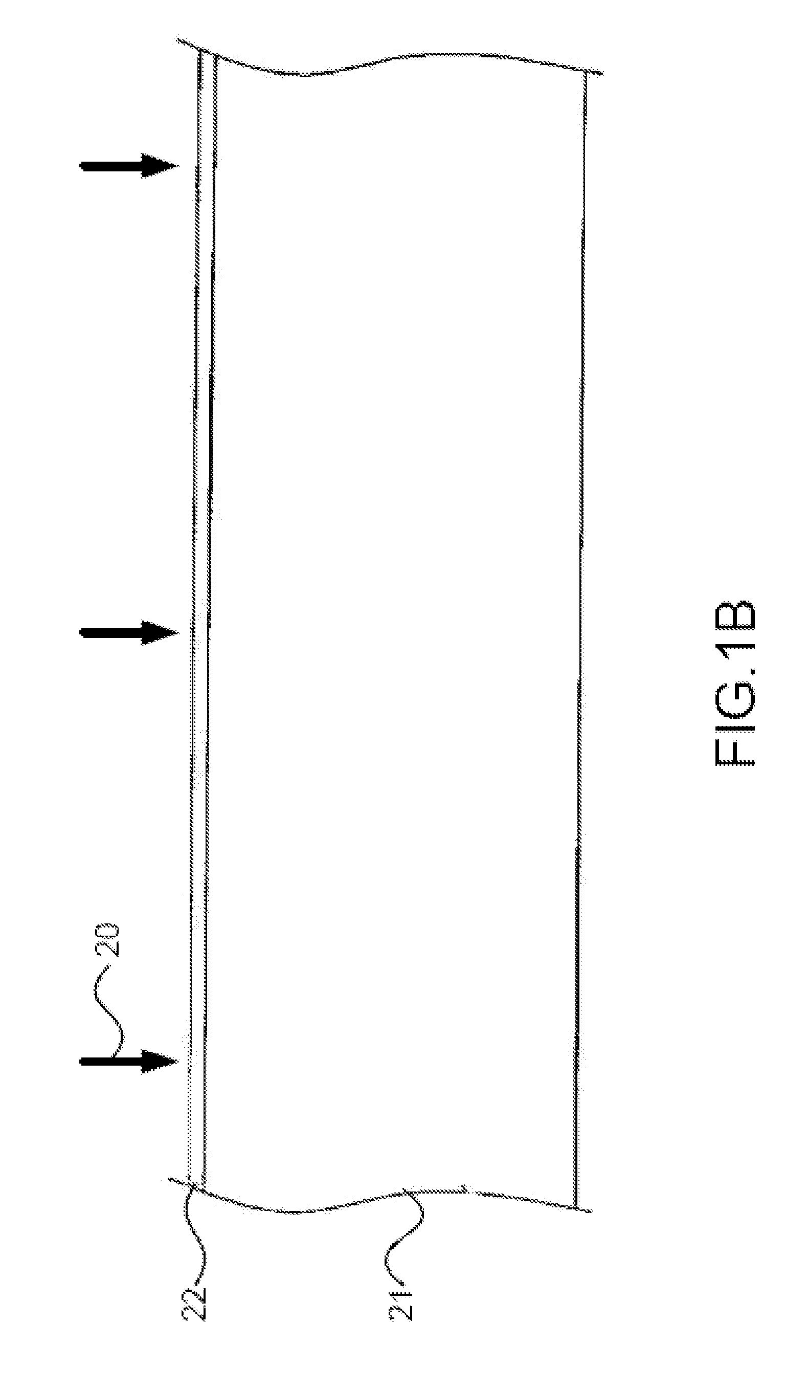
[0028](a) Forming barrier pattern 11: In FIG. 1B and FIG. 1C, a barrier pattern...
PUM
 Abstract
Description
Claims
Application Information