

Voltage regulator circuit
a voltage regulator and circuit technology, applied in the direction of dc-dc conversion, power conversion systems, instruments, etc., can solve the problems of low on-off ratio of thin film transistors, stoichiometric composition differences in oxide semiconductors, etc., to achieve the conversion efficiency to obtain the desired voltage, reduce leakage current of transistors, and improve the effect of output voltage drop
- Summary
- Abstract
- Description
- Claims
- Application Information
AI Technical Summary
Benefits of technology
Problems solved by technology
Method used
Image

Examples
embodiment 1
[0045]In this embodiment, a voltage regulator circuit which is an embodiment of the present invention will be described.
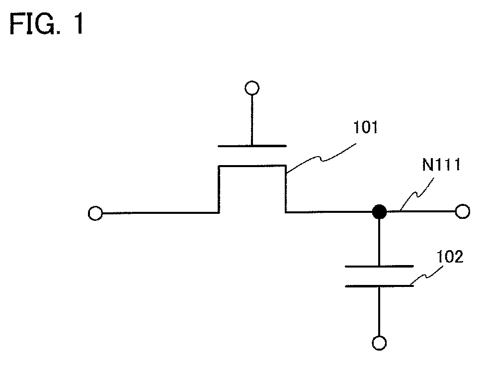
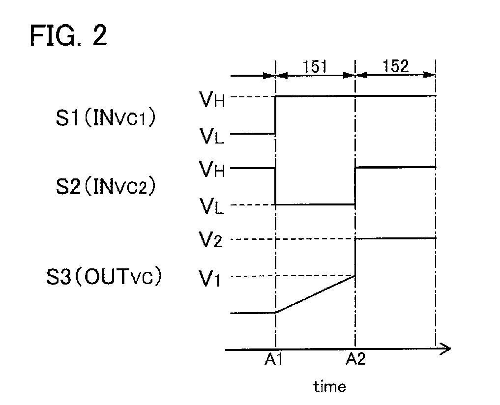
[0046]An example of a structure of a voltage regulator circuit described in this embodiment has a function of inputting a signal S1 and a signal S2 as input signals, stepping up or stepping down the voltage of the input signal S1, and thereby outputting as an output signal a signal S3 which has a voltage obtained by stepping up or stepping down the voltage of the signal S1. An example of the structure of the voltage regulator circuit in this embodiment is further described with reference to FIG. 1. FIG. 1 is a circuit diagram illustrating an example of the structure of the voltage regulator circuit of this embodiment.
[0047]The voltage regulator circuit illustrated in FIG. 1 includes a transistor 101 and a capacitor 102.
[0048]In this specification, for example, a field-effect transistor can be used as the transistor.
[0049]In addition, in this specification, the fiel...
embodiment 2
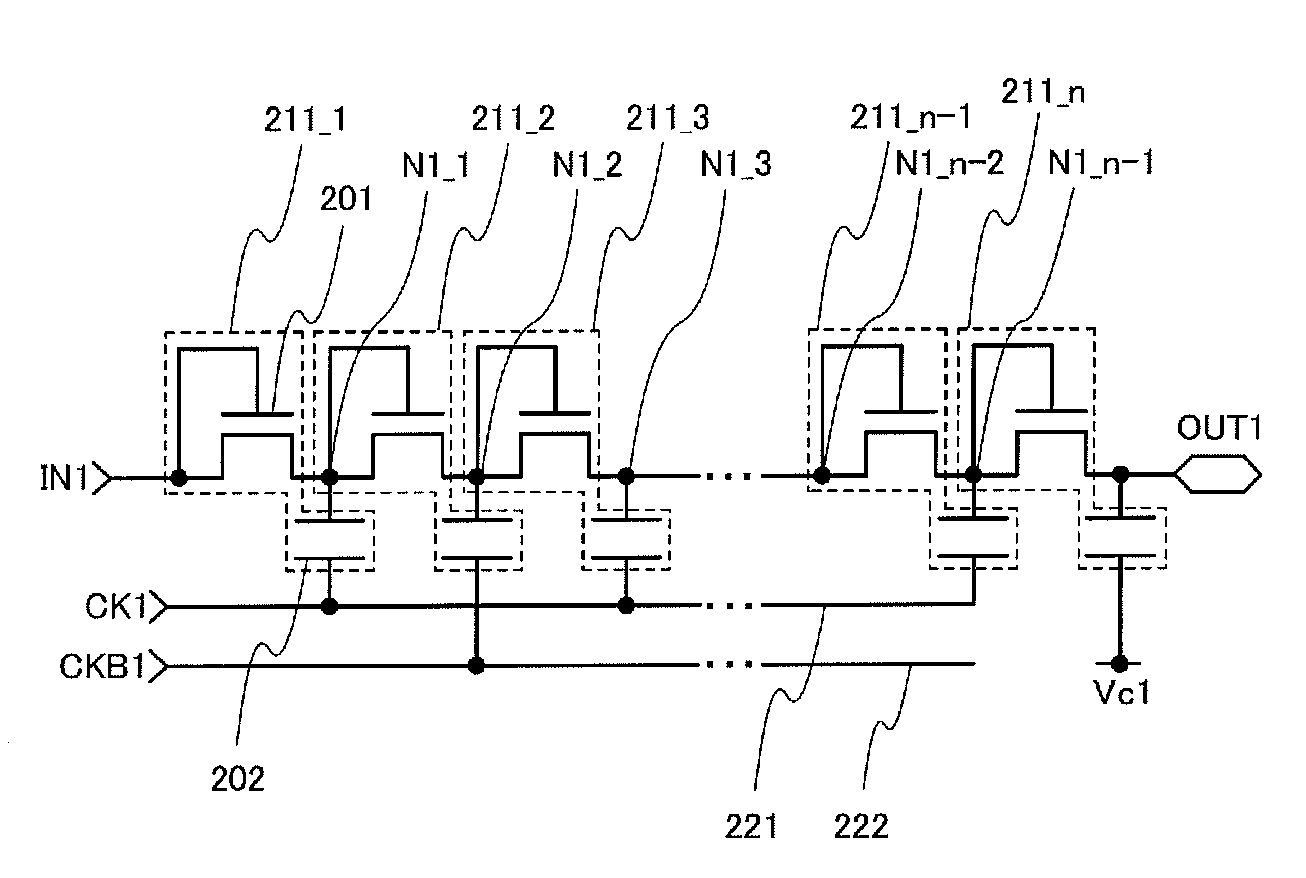
[0073]In this embodiment, a step-up circuit will be described as an example of a voltage regulator circuit which is an embodiment of the present invention.
[0074]An example of the circuit structure of a voltage regulator circuit according to this embodiment will be described with reference to FIG. 3. FIG. 3 is a circuit diagram illustrating an example of the circuit structure of a voltage regulator circuit according to this embodiment.
[0075]The voltage regulator circuit illustrated in FIG. 3 includes a unit step-up circuit 211_1 to a unit step-up circuit 211—n (n is a natural number of greater than or equal to 2) and is formed with n stages of unit step-up circuits obtained by electrically connecting the unit step-up circuit 211_1 to the unit step-up circuit 211—n in series.
[0076]The unit step-up circuits 211_1 to 211—n each include a transistor 201 and a capacitor 202.
[0077]As the transistor 201, a transistor which includes an oxide semiconductor layer serving as a channel formation...
embodiment 3
[0098]In this embodiment, a step-down circuit will be described as another example of a voltage regulator circuit which is an embodiment of the present invention. Note that in this embodiment, the description in Embodiment 2 is employed as appropriate for the same portions as the voltage regulator circuit in Embodiment 2.
[0099]An example of the circuit structure of a voltage regulator circuit in this embodiment is described with reference to FIG. 4. FIG. 4 is a circuit diagram illustrating an example of the circuit structure of a voltage regulator circuit in this embodiment.
[0100]The voltage regulator circuit illustrated in FIG. 4 includes a unit step-down circuit 511_1 to a unit step-down circuit 511—n (n is a natural number of greater than or equal to 2) and is formed with n stages of unit step-down circuits obtained by electrically connecting the unit step-down circuit 511_1 to the unit step-down circuit 511—n in series.
[0101]The unit step-down circuits 511_1 to 511—n each includ...
PUM
 Abstract
Description
Claims
Application Information