Phase calibration circuit, memory card control device, and phase calibration method

a phase calibration and memory card control technology, applied in the field of memory card control devices, can solve the problems of increasing processing speed, difficult registration, and inability to address the variation of the propagation delay of read-out data, and achieve the effect of suppressing the degradation of transfer efficiency

Inactive Publication Date: 2011-04-21
RENESAS ELECTRONICS CORP
View PDF12 Cites 21 Cited by
  • Summary
  • Abstract
  • Description
  • Claims
  • Application Information

AI Technical Summary

Benefits of technology

[0018]According to an exemplary aspect of the present invention, it is possible to su

Problems solved by technology

However, because the transfer clock signal supplied to the memory card and the clock signal to acquire read-out data are the same, it is difficult to perform a registration.
This registration becomes more difficult with increasing processing speed.
However a memory controller disclosed in Japanese Unexamined Patent Application Publication No. 2004-192488 cannot address propagation delay variation of the read-out data caused by variation of voltage or

Method used


Image

  • Phase calibration circuit, memory card control device, and phase calibration method
  • Phase calibration circuit, memory card control device, and phase calibration method
  • Phase calibration circuit, memory card control device, and phase calibration method

Examples


first exemplary embodiment

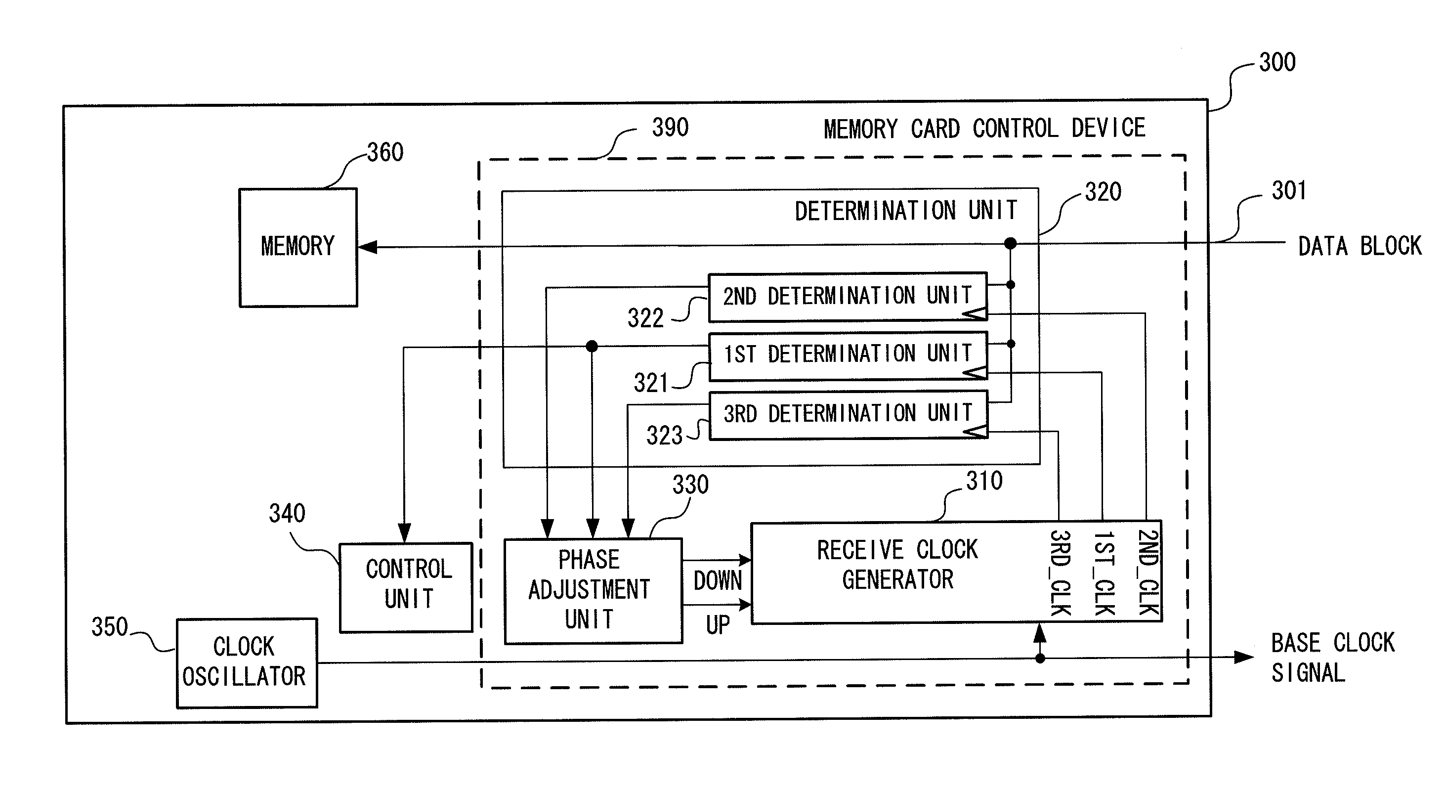
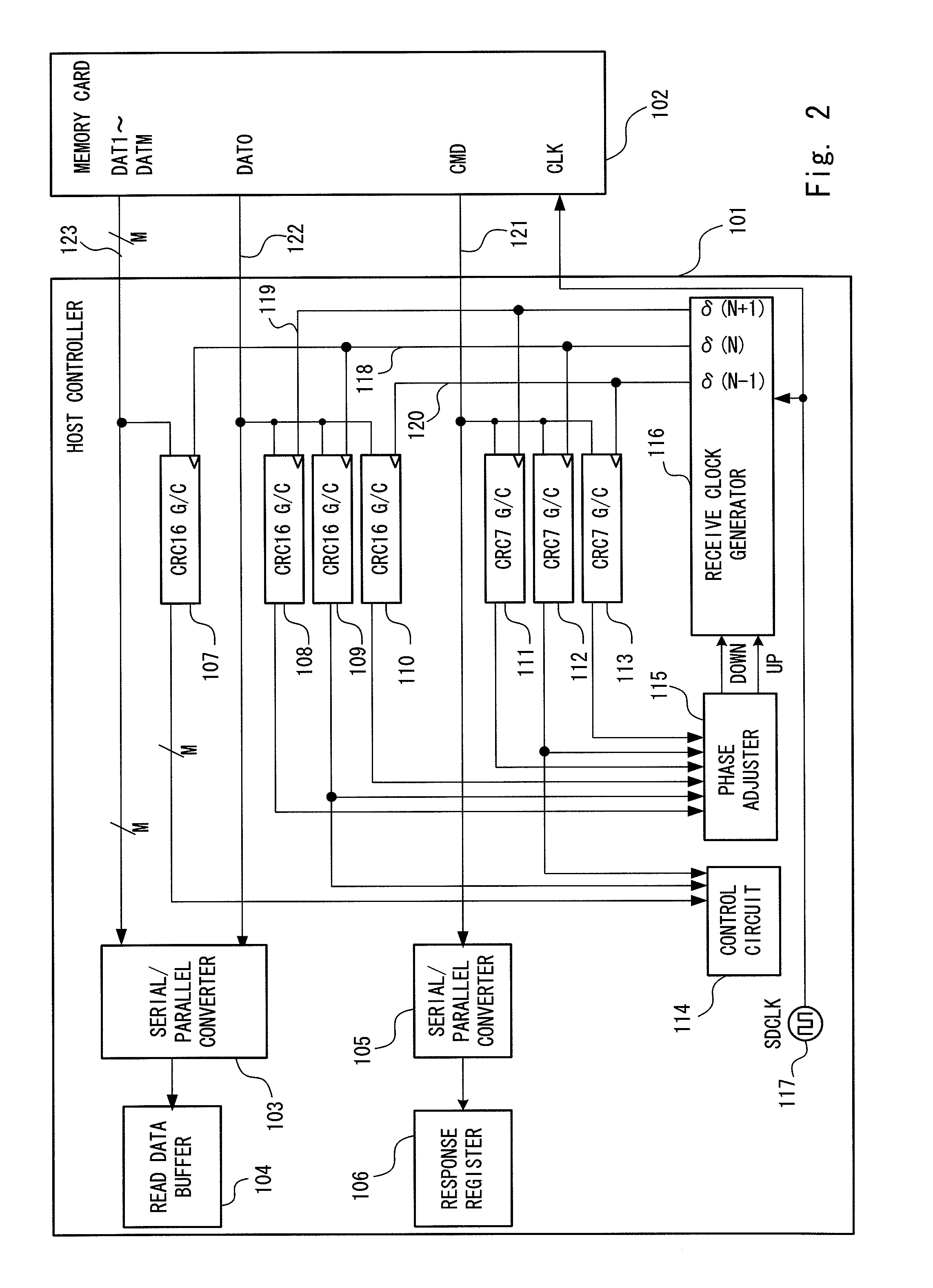
[0044]A first exemplary embodiment describes a case where redundant data as the detection information for detecting an error is appended to the data body transferred from the memory card, and specifically the CRC code appended to the data block, for example.

[0045]FIG. 2 is a block diagram showing an exemplary configuration of a memory card control device (host controller) according to the first exemplary embodiment of this invention. FIG. 2 shows an exemplary configuration of a host controller 101 as a specific example of the memory card control device 300 shown in FIG. 1. FIG. 2 also shows a memory card 102 for clarifying a relationship between the host controller 101 and the memory card 102. The host controller 101 transmits and receives the data block to / from the memory card 102. In the following explanation, the response data is transferred via a bus 121 connected to a terminal CMD of the memory card 102, and the read data is transferred via buses 122 and 123 connected to termin...

second exemplary embodiment

[0090]While the first exemplary embodiment employs the memory card which uses CRC codes as the error detection method for the data block, such as the MMC or the SD card, a calibration system of this invention can be easily applied to a data block transfer means which uses different error detection method. For example, an error detection method which uses a data block represented by a format including a data body (such as RD1 shown in FIG. 4) and a redundant block (RD2) calculated by the data body may be used. It is possible to use general error detecting code or a portion of error correcting codes. In particular, a parity code, a check sum, a hash value, or the like may be used as the error detecting code. A BCH code, a hamming code, or the like may be used as an error correcting code. Instead of using the method to append redundant data such as the error correcting code as described above, other methods may be used such as a method to use error correcting codes which enable to info...

third exemplary embodiment

[0091]In the first exemplary embodiment, a synchronous memory card is assumed, but this invention may be easily applied to a device and a method which employ a memory specification where a data output delay from the memory card is specified by more than one clock cycle. For example, it is assumed that a phase adjustment range is 360°. In this case, even when there is no correlation between a data output delay and an operation clock signal, it is possible to receive data by adjusting a sampling point to an arbitrary angle by setting the phase adjustment range to 360°. Further, even when the data output delay wobbles, it is possible to correct the phase of the receive clock signal and to continue data reception.

Other Exemplary Embodiments

[0092]Although the case where the receive clock generator 310 (receive clock generator 116) uses the three receive clock signals is explained in each of the exemplary embodiment, the receive clock generator 310 may generate more than three clock signa...


PUM


Abstract

Provided is a phase calibration circuit to suppress degradation of transfer efficiency when reading data from a memory card. The phase calibration circuit includes a receive clock generator that generates clock signals including a first clock signal (FCS) with a phase shifted with respect to a base clock signal, a second clock signal with a phase advanced with respect to the FCS, and a third clock signal with a phase delayed with respect to the FCS; a determination unit that acquires data blocks, each of which including a data body and detection information for detecting an error, in accordance with the clock signals, determines whether an error occurs by using the detection information of the data blocks, and outputs determination results; and a phase adjustment unit that instructs the receive clock generator to adjust a phase of the FCS depending on the determination results.

Description

INCORPORATION BY REFERENCE[0001]This application is based upon and claims the benefit of priority from Japanese patent application No. 2009-241115, filed on Oct. 20, 2009, the disclosure of which is incorporated herein in its entirety by reference.BACKGROUND[0002]1. Field of the Invention[0003]This invention relates to a memory card control device, and particularly to a phase calibration circuit and a phase calibration method to perform clock control when reading data from a memory card.[0004]2. Description of Related Art[0005]A memory card control device (which is also referred to hereinafter as “host controller”) supplies a transfer clock signal (base clock signal) for communicating data with the memory card. The memory card communicates data with the memory card control device based on the transfer clock signal that is received. When reading data from the memory card, the host controller acquires data transferred from the memory card in accordance with a clock signal synchronized...

Claims


Application Information

Patent Timeline
IPC IPC(8): G06F11/10H03L7/06G06F11/07
CPCG06F11/1004H03L7/087H03L7/0814G06F2213/0038
Inventor TAKAGI, KENICHI
Owner RENESAS ELECTRONICS CORP
Why Eureka
Try Eureka