Esd/antenna diodes for through-silicon vias

a technology of through-silicon vias and diodes, which is applied in the direction of cad circuit design, computer aided design, instruments, etc., can solve the problems of gate dielectrics being subject to a risk of breakdown, affecting the performance of circuits, etc., to achieve more powerful circuits, components and systems, and improve chip yields

Active Publication Date: 2011-04-28
SYNOPSYS INC
View PDF32 Cites 45 Cited by
  • Summary
  • Abstract
  • Description
  • Claims
  • Application Information

AI Technical Summary

Benefits of technology

[0017]A need therefore exists for a robust solution to the problem of charge pickup by TSVs during the integrated c...

Problems solved by technology

But since conductive paths are often routed in such a way that they jump among different metal layers, the connection of a transistor gate terminal to a driver often is not completed until higher layers of metal are formed on the wafer.
During these time periods, the gate dielectrics are subject to a risk of breakdown due to charge buildup on the M1 conductor to which it is connected.
There is a related source of plasma induced gate oxide damage which occurs during fabrication, referred to herein as “antenna effect electrostatic discharge (ESD) damage.” This problem occurs because during fabrication some M1 conductors are connected through contacts to the drain diffusion or implant of N-channel transistors, thereby providing another path for charge built up on the conductors to break down gate dielectrics as it couples to the gate poly.
On the other hand, this solution places a heavy burden on routing software.
On the other hand, the requirement for two vias for every gate undesirably occupies valuable chip area.
The use of antenna diodes as in the third and fourth solutions above, can avoid the problems of the first and second solutions, but they undesirably occupy val...

Method used


Image

  • Esd/antenna diodes for through-silicon vias
  • Esd/antenna diodes for through-silicon vias
  • Esd/antenna diodes for through-silicon vias

Examples


Embodiment Construction

[0039]The following description is presented to enable any person skilled in the art to make and use the invention, and is provided in the context of a particular application and its requirements. Various modifications to the disclosed embodiments will be readily apparent to those skilled in the art, and the general principles defined herein may be applied to other embodiments and applications without departing from the spirit and scope of the present invention. Thus, the present invention is not intended to be limited to the embodiments shown, but is to be accorded the widest scope consistent with the principles and features disclosed herein.

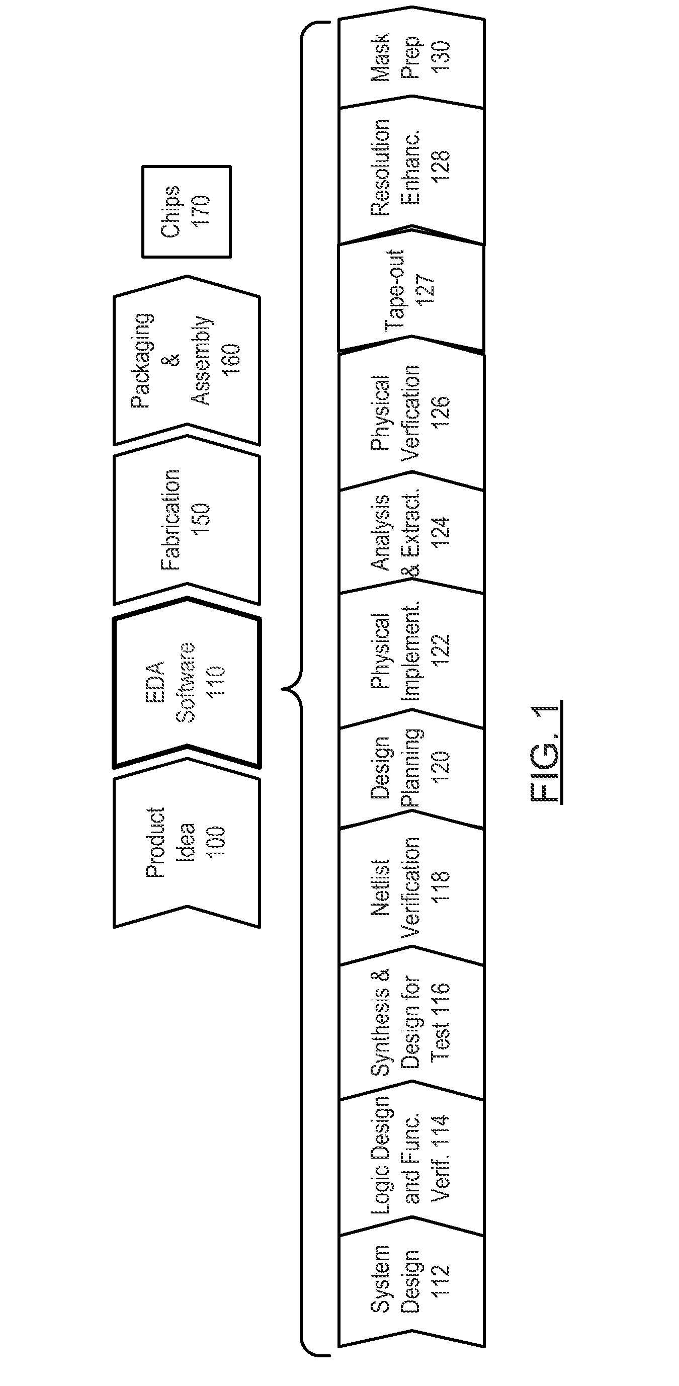
[0040]FIG. 1 shows a simplified representation of an illustrative digital integrated circuit design flow. At a high level, the process starts with the product idea (step 100) and is realized in an EDA (Electronic Design Automation) software design process (step 110). When the design is finalized, it can be taped-out (step 127). At some point af...


PUM


Abstract

Roughly described, an antenna diode is formed at least partially within the exclusion zone around a TSV, and is connected to the TSV by way of a metal 1 layer conductor at the same time that the TSV is connected to either the gate poly or a diffusion region of one or more transistors placed outside the exclusion zone.

Description

BACKGROUND[0001]The present invention relates to methods and structures for addressing ESD and antenna effects experienced by devices in the presence of through-silicon vias.[0002]Finished integrated circuit devices typically include diffusions and implant regions in the body of a silicon wafer. Above the silicon itself is a gate dielectric layer (such as an oxide), and above that a gate layer in which transistor gates are patterned. The gate layer is usually polysilicon, but in some fabrication processes it can be metal. Above that are several layers of metal interconnects, each separated from the previous layer by a dielectric. Where interconnections are required from one layer to another, an opening is formed through the intervening dielectric layer and filled with a conductive material. There are many variations on this structure, but the one just described is common.[0003]The interconnections between layers are referred to as ‘vias’ if they interconnect two metal interconnect l...

Claims


Application Information

Patent Timeline
IPC IPC(8): H01L27/06G06F17/50H01L21/336
CPCH01L23/481H01L23/60H01L23/62H01L27/0255H01L2225/06541H01L2924/0002G06F17/5068H01L27/0207H01L2924/00012H01L2924/00H01L23/48G06F30/39
Inventor SU, QINGNI, MINTANG, ZONGWUKAWA, JAMILSPROCH, JAMES D.
Owner SYNOPSYS INC
Why Eureka
Try Eureka