Power diode, rectifier, and semiconductor device including the same

a technology of rectifier and diode, which is applied in the direction of diodes, semiconductor devices, electrical apparatus, etc., to achieve the effects of small reverse saturation current, and high withstand voltag

Inactive Publication Date: 2011-05-05
SEMICON ENERGY LAB CO LTD
View PDF99 Cites 23 Cited by
  • Summary
  • Abstract
  • Description
  • Claims
  • Application Information

AI Technical Summary

Benefits of technology

[0006]As described above, although a diode in which silicon carbide is used is expected to have high withstand voltage and small reverse saturation current, there are many problems in manufacturing and achieving such an element.
[0007]In view of the above, it is an object of an embodiment of the present invention to provide a power diode or a rectifier including a diode with small reverse saturation current. In addition, it is an object to manufacture a diode with small reverse saturation current at low process temperature (e.g., less than or equal to 800° C.) and to provide a power diode or a rectifier including the diode.
[0008]An embodiment of the present invention provides a power diode and a rectifier including a diode which can be miniaturized and includes a field-effect transistor, for example, a thin film transistor that can be manufactured at low process temperature and has large on-state current and small off-state current. The diode includes a first electrode provided over a substrate, an oxide semiconductor film provided on and in contact with the first electrode and purified, a second electrode provided on and in contact with the oxide semiconductor film, a gate insulating film covering the first electrode, the oxide semiconductor film, and the second electrode, and third electrodes provided in contact with the gate insulating film and facing each other with the first electrode, the oxide semiconductor film, and the second electrode interposed therebetween or a third electrode provided in contact with the gate insulating film and surrounding the second electrode. In the non-linear element, the third electrodes or the third electrode are / is connected to the first electrode or the second electrode, and a current flows between the first electrode and the second electrode.
[0009]A power diode capable of conducting a larger amount of current than a conventional power diode can be obtained.
[0010]A rectifier having a higher withstand voltage than a conventional rectifier can be obtained.

Problems solved by technology

As described above, although a diode in which silicon carbide is used is expected to have high withstand voltage and small reverse saturation current, there are many problems in manufacturing and achieving such an element.

Method used


Image

  • Power diode, rectifier, and semiconductor device including the same
  • Power diode, rectifier, and semiconductor device including the same
  • Power diode, rectifier, and semiconductor device including the same

Examples


embodiment 1

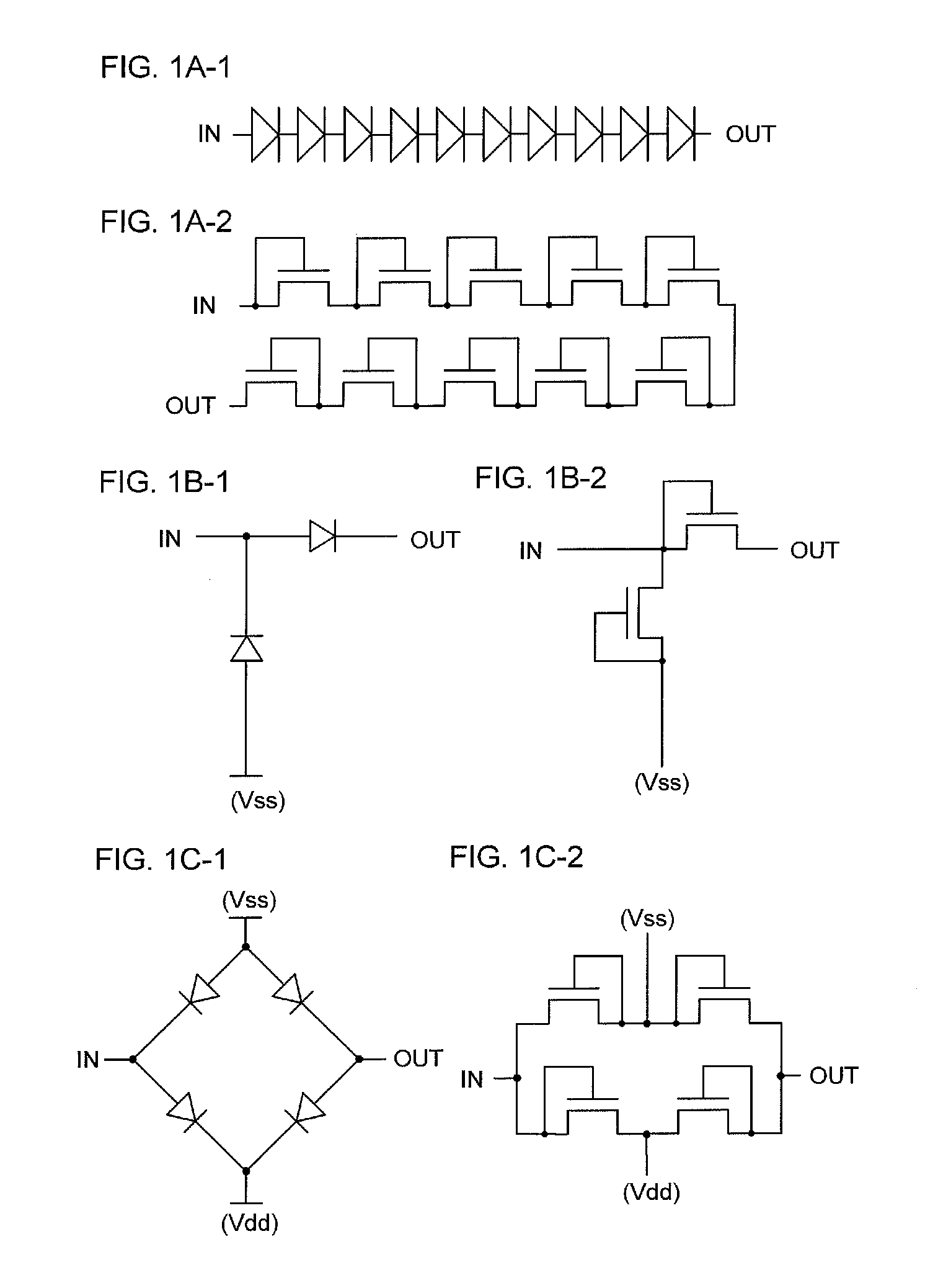
[0026]In this embodiment, examples of structures of a power diode and a rectifier which are embodiments of the present invention will be described with reference to FIGS. 1A-1, 1A-2, 1B-1, 1B-2, 1C-1, and 1C-2.

[0027]FIG. 1A-1 illustrates an example of a structure of a power diode which is one embodiment of the present invention. In the power diode illustrated in FIG. 1A-1, a plurality of diodes is connected in series in a forward direction.

[0028]FIG. 1B-1 illustrates an example of a structure of a rectifier which is one embodiment of the present invention. The rectifier illustrated in FIG. 1B-1 is a half-wave rectifier including two diodes. An anode of a first diode is connected to a lower potential side reference potential (preferably, a ground potential). A cathode of the first diode is connected to an input portion and an anode of a second diode. A cathode of the second diode is connected to an output portion.

[0029]FIG. 1C-1 illustrates an example of a structure of a rectifier wh...

embodiment 2

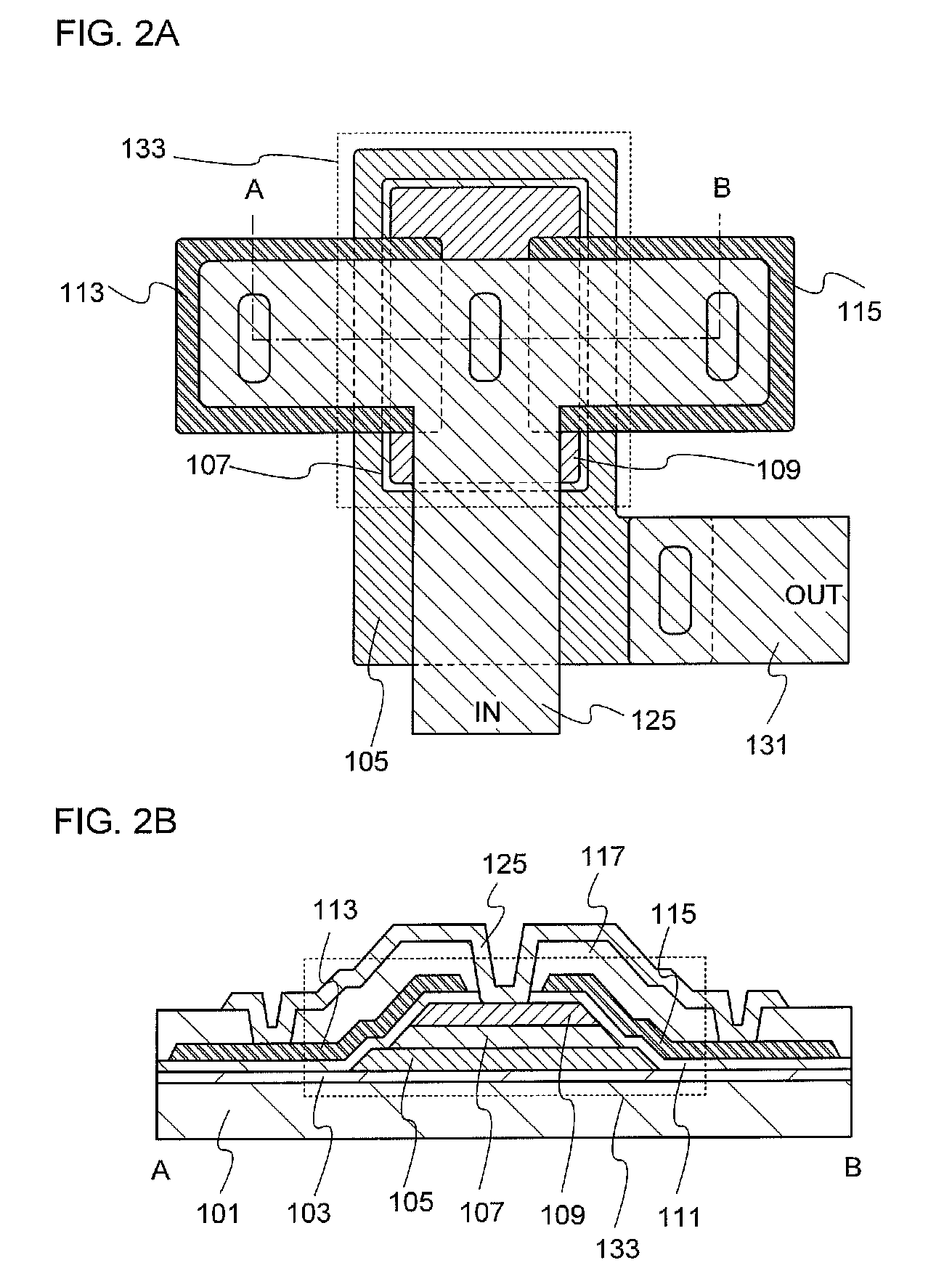
[0060]In this embodiment, an example of a diode, which can be applied to a power diode and a rectifier of embodiments of the present invention and which has a structure different from that in Embodiment 1, will be described with reference to FIGS. 4A and 4B. The diode which is described in this embodiment can be obtained by connecting a source or a drain of a field-effect transistor, including a thin film transistor to a gate thereof.

[0061]In the diode illustrated in FIGS. 4A and 4B, a wiring 131 is connected to a first electrode 105 and a third electrode 113, and a wiring 132 is connected to a first electrode 106 and a third electrode 115. The first electrode 105 and the first electrode 106 are connected to a second electrode 109 through an oxide semiconductor film 107. The second electrode 109 is connected to a wiring 129.

[0062]FIG. 4A is a top view of diode-connected thin film transistors 141 and 143. FIG. 4B is a cross-sectional view along dashed-and-dotted line A-B in FIG. 4A.

[...

embodiment 3

[0075]In this embodiment, an example of a diode, which can be applied to a power diode and a rectifier of embodiments of the present invention and which has a structure different from those in Embodiments 1 and 2, will be described with reference to FIGS. 6A and 6B. The diode which is described in this embodiment can be obtained by connecting a source or a drain of a field-effect transistor, including a thin film transistor to a gate thereof.

[0076]In the diode illustrated in FIGS. 6A and 6B, a wiring 131 is connected to a first electrode 105 and a third electrode 113. The first electrode 105 is connected to a second electrode 109 through an oxide semiconductor film 107. The second electrode 109 is connected to a wiring 129.

[0077]FIG. 6A is a top view of a diode-connected thin film transistor 145. FIG. 6B is a cross-sectional view along dashed-and-dotted line A-B in FIG. 6A.

[0078]As illustrated in FIG. 6B, the first electrode 105, the oxide semiconductor film 107, and the second elec...


PUM


Abstract

With a non-linear element (e.g., a diode) with small reverse saturation current, a power diode or rectifier is provided. A non-linear element includes a first electrode provided over a substrate, an oxide semiconductor film provided on and in contact with the first electrode and having a concentration of hydrogen of 5×10¹⁹ atoms/cm3 or less, a second electrode provided on and in contact with the oxide semiconductor film, a gate insulating film covering the first electrode, the oxide semiconductor film, and the second electrode, and third electrodes provided in contact with the gate insulating film and facing each other with the first electrode, the oxide semiconductor film, and the second electrode interposed therebetween or a third electrode provided in contact with the gate insulating film and surrounding the second electrode. The third electrodes are connected to the first electrode or the second electrode. With the non-linear element, a power diode or a rectifier is formed.

Description

TECHNICAL FIELD[0001]The present invention relates to a power diode and a rectifier including a non-linear element using an oxide semiconductor. Furthermore, the present invention relates to a semiconductor device including the power diode or the rectifier.BACKGROUND ART[0002]Among semiconductor devices, diodes are required to have high withstand voltage, small reverse saturation current, and the like. In order to meet such a requirement, a diode in which silicon carbide (SiC) is used has been researched. Silicon carbide used as a semiconductor material has a width of a forbidden band of 3 eV or more, excellent controllability of electric conductivity at high temperature, and is more resistant to dielectric breakdown than silicon. Therefore, silicon carbide is expected to be applied to a diode in which reverse saturation current is small and withstand voltage is high. For example, a Schottky barrier diode in which silicon carbide is used and reverse leakage current is reduced is kno...

Claims


Application Information

Patent Timeline
Patent Type & Authority Applications(United States)
IPC IPC(8): H01L29/22
CPCH01L29/22H01L29/24H01L29/7391H01L27/0629H01L29/7869H01L27/1225H01L27/0605H01L29/78642H01L29/66969
Inventor YAMAZAKI, SHUNPEI
Owner SEMICON ENERGY LAB CO LTD
Why Eureka
Try Eureka