Fast recovery diode

a diode and fast recovery technology, applied in the field of power electronics, can solve the problems of large differences in other relevant device parameters, and achieve the effect of fast recovery and fast recovery

a diode and fast recovery technology, applied in the field of power electronics, can solve the problems of large differences in other relevant device parameters, and achieve the effect of fast recovery and fast recovery

US20110108941A1Active Publication Date: 2011-05-12HITACHI ENERGY SWITZERLAND AG

Image

  • Fast recovery diode
  • Fast recovery diode
  • Fast recovery diode

Examples


Embodiment Construction

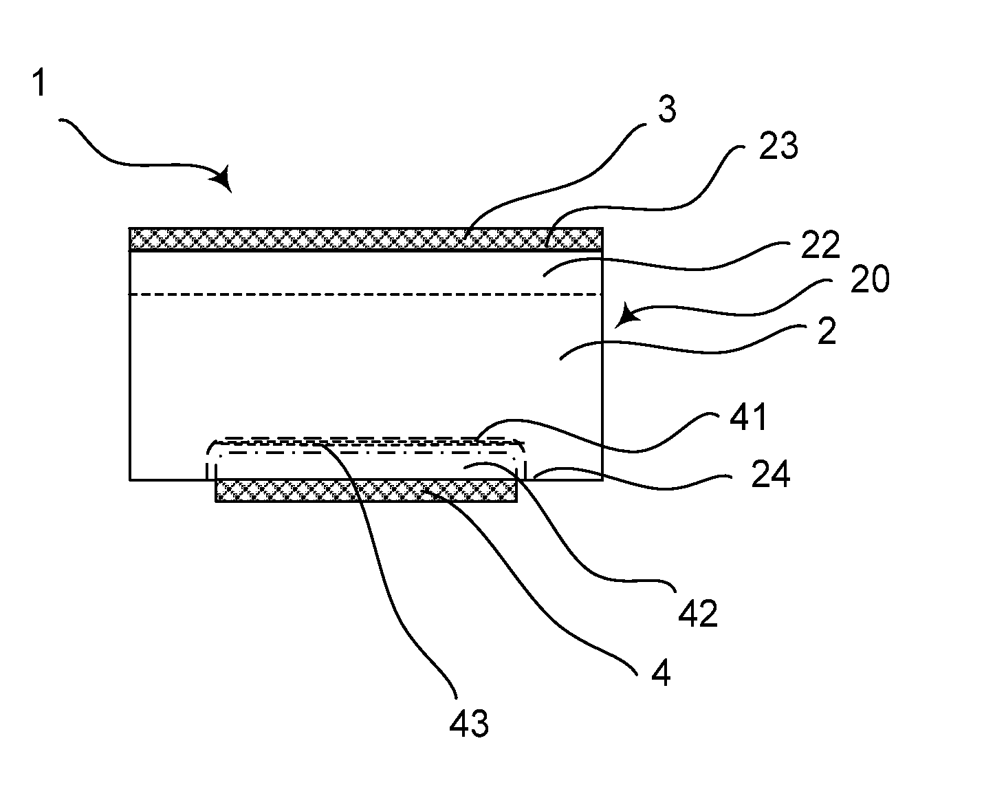
[0017]Exemplary embodiments of the present disclosure provide a fast recovery diode with lower switching losses and lower reverse leakage current and therefore a higher thermal operation range than known devices. In addition, exemplary embodiments of the present disclosure provide a manufacturing method for such a device.

[0018]According to an exemplary embodiment, the fast recovery diode includes a base layer of a first conductivity type with a cathode side and an anode side opposite the cathode side. An anode buffer layer of a second conductivity type with a first depth and a first maximum doping concentration is arranged on the anode side. By this anode buffer layer, the electric field is stopped during reverse bias before it reaches the defect layer.

[0019]An anode contact layer of the second conductivity type with a second depth, which is lower than the first depth, and a second maximum doping concentration, which is higher than the first maximum doping concentration, is arranged...


PUM


Abstract

A fast recovery diode includes a base layer of a first conductivity type. The base layer has a cathode side and an anode side opposite the cathode side. An anode buffer layer of a second conductivity type having a first depth and a first maximum doping concentration is arranged on the anode side. An anode contact layer of the second conductivity type having a second depth, which is lower than the first depth, and a second maximum doping concentration, which is higher than the first maximum doping concentration, is also arranged on the anode side. A space charge region of the anode junction at a breakdown voltage is located in a third depth between the first and second depths. A defect layer with a defect peak is arranged between the second and third depths.

Description

RELATED APPLICATION[0001]This application claims priority under 35 U.S.C. §119 to European Patent Application No. 09175419.2 filed in Europe on Nov. 9, 2009, the entire content of which is hereby incorporated by reference in its entirety.FIELD[0002]The present disclosure relates to the field of power electronics. More particularly, the present disclosure relates to a fast recovery diode, and to a method for manufacturing such a fast recovery diode.BACKGROUND INFORMATION[0003]As shown in FIG. 1, a known diode 10 includes an n-doped base layer 2 having a cathode side 23 and an anode side 24 opposite the cathode side 23. On the anode side 24, a p-doped anode layer 25 is arranged, and a metal layer which functions as an anode electrode 4 is arranged on top of the p-doped anode layer 25 . A higher (n+) doped cathode buffer layer 22 is arranged on the cathode side 23. A metal layer in form of a cathode electrode 3 is arranged on top of the (n+) doped cathode buffer layer 22. On the anode ...

Claims


Application Information

Patent Timeline
12 May 2011
Publication
US20110108941A1
IPC
H01L29/872; H01L29/87; H01L29/739; H01L21/266
CPC
H01L29/32; H01L29/861; H01L29/66136
Inventors
VOBECKY, JAN; KOPTA, ARNOST