Low temperature ceramic microelectromechanical structures

a microelectromechanical and low temperature technology, applied in the field of manufacturing mems devices, can solve the problems of power consumption, process variability, and difficulty in gearing the mems fabrication process towards general applications, and achieve the effect of reducing power consumption, reducing manufacturing costs, and improving manufacturing efficiency

Active Publication Date: 2011-05-12
MCGILL UNIV
View PDF5 Cites 34 Cited by
  • Summary
  • Abstract
  • Description
  • Claims
  • Application Information

AI Technical Summary

Benefits of technology

[0015]In accordance with the invention there is provided a method comprising a substrate, and providing at least a low temperature deposited MEMS structure comprising at least two MEMS elements, the two MEMS eleme

Problems solved by technology

However, because of this vast range of functionality, MEMS fabrication processes, unlike the microelectronics industry, are difficult to gear towards general applications.
As a result most processes are aimed at the fabrication of a few devices, and usually performance of the devices is hindered by process variability.
This is essentially because of the unparalleled benefits available from CMOS in the areas of circuit size, operating speed, energy efficiency and manufacturing costs which continue to improve from the geometric downsizing that comes with every new generation of semiconductor manufacturing processes.
This power consumption arising from the charging and discharging of various load capacitances within the CMOS circuits, mostly gate and wire capacitance, but also transistor drain and transistor source capacitances, whenever they are switched.
However, combining CMOS and MEMS technologies has been especially ch

Method used


Image

  • Low temperature ceramic microelectromechanical structures
  • Low temperature ceramic microelectromechanical structures
  • Low temperature ceramic microelectromechanical structures

Examples


Embodiment Construction

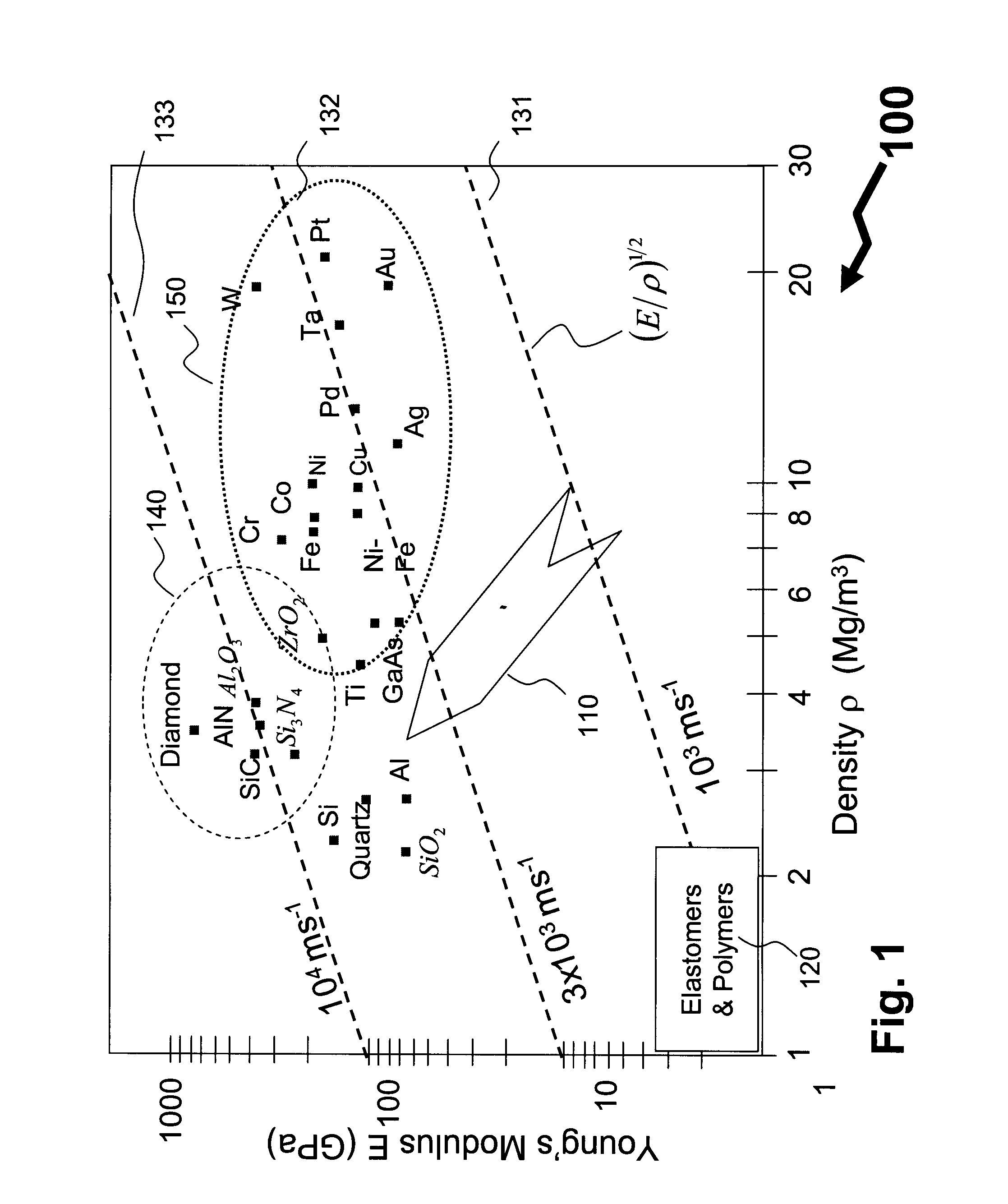
[0035]Referring to FIG. 1 shown is a material selection chart 100 for MEMS device implementations. Plotted onto the material selection chart are a range of different materials including metals, dielectrics, ceramics and polymers. Each material being represented by a point on the X-Y graph wherein the X-axis is density and Young's modulus is the Y-axis. The data being plotted is according to the work of V. T. Srikar et al “Materials Selection in Micro-Mechanical Design: An Application of the Ashby Approach” (J. Microelectromechanical Systems Vol. 10, No. 1, pp. 3-10). As acoustic velocity, a factor governing the resonant frequency of structural materials, is determined in accordance to Equation 2 below shown are lines of constant acoustic velocity 131, 132, 133 of 1×10³ ms−1, 3×10³ ms−1, and 1×10⁴ ms−1 respectively.

υ=Eρ.(2)

[0036]As evident from the material selection chart, different types of materials tend to be grouped together. Ceramic materials 140 tending to appear in the top le...


PUM


Abstract

A method of providing microelectromechanical structures (MEMS) that are compatible with silicon CMOS electronics is provided. The method providing for processes and manufacturing sequences limiting the maximum exposure of an integrated circuit upon which the MEMS is manufactured to below 350° C., and potentially to below 250° C., thereby allowing direct manufacturing of the MEMS devices onto electronics, such as Si CMOS circuits. The method further providing for the provisioning of MEMS devices with multiple non-conductive structural layers such as silicon carbide separated with small lateral gaps. Such silicon carbide structures offering enhanced material properties, increased environmental and chemical resilience whilst also allowing novel designs to be implemented taking advantage of the non-conductive material of the structural layer. The use of silicon carbide being beneficial within the formation of MEMS elements such as motors, gears, rotors, translation drives, etc where increased hardness reduces wear of such elements during operation.

Description

CROSS-REFERENCE TO RELATED APPLICATIONS[0001]This application claims the benefit of priority to U.S. Provisional Patent Application Ser. No. 61 / 129,644 filed Jul. 9, 2008 entitled “Low Temperature Ceramic MicroElectroMechanical Structures”.FIELD OF THE INVENTION[0002]The invention relates to manufacturing MEMS devices and more particularly to manufacturing and designing MEMS devices with lateral features and metallization for integration directly with integrated electronic circuits.BACKGROUND OF THE INVENTION[0003]Microelectromechanical systems (MEMS) are small integrated devices or systems that combine electrical and mechanical components. The components can range in size from the sub-micrometer level to the millimeter level, and there can be any number, from one, to few, to potentially thousands or millions, in a particular system. Historically MEMS devices have leveraged and extended the fabrication techniques developed for the silicon integrated circuit industry, namely lithogra...

Claims


Application Information

Patent Timeline
IPC IPC(8): H01L21/02
CPCB81B2201/0235B81C2203/0721B81C1/00063B81B3/0021B81C2203/0735B81C2201/0174B81C2201/0169B81C2201/014B81C1/00666B81C1/00587B81C1/00396B81C1/00246B81B2207/03B81B2201/03B81B2201/0271B81B2201/01B81B7/008B81B2207/015
Inventor EL-GAMAL, MOURAD
Owner MCGILL UNIV
Why Eureka
Try Eureka