

Wafer bonding method
a bonding method and bonding technology, applied in the field of bonding methods, can solve the problems of insufficient void reduction and contamination of organic substances, and achieve the effect of further reducing the surface roughness of the cvd oxide film
- Summary
- Abstract
- Description
- Claims
- Application Information
AI Technical Summary
Benefits of technology
Problems solved by technology
Method used
Image

Examples
embodiments
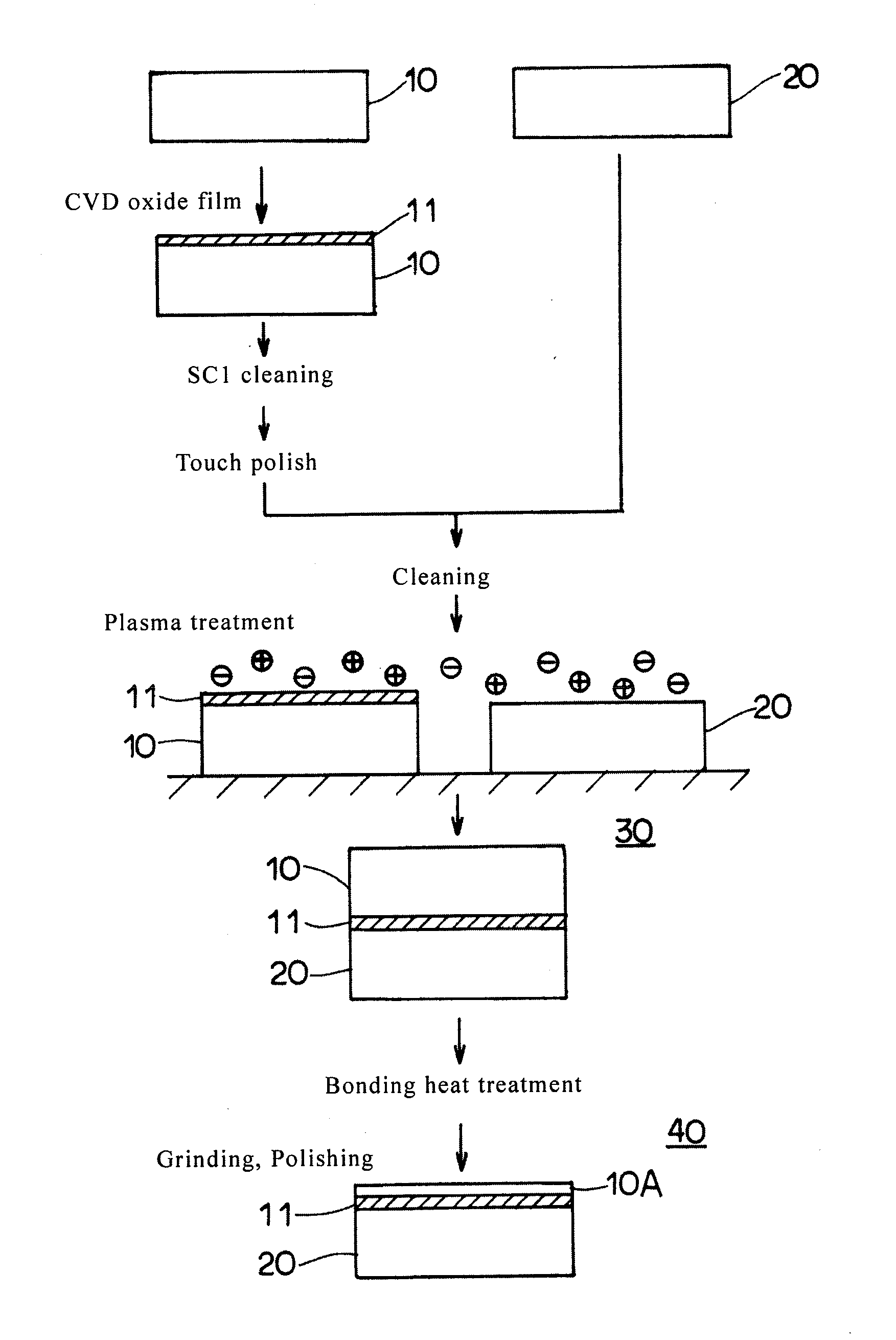
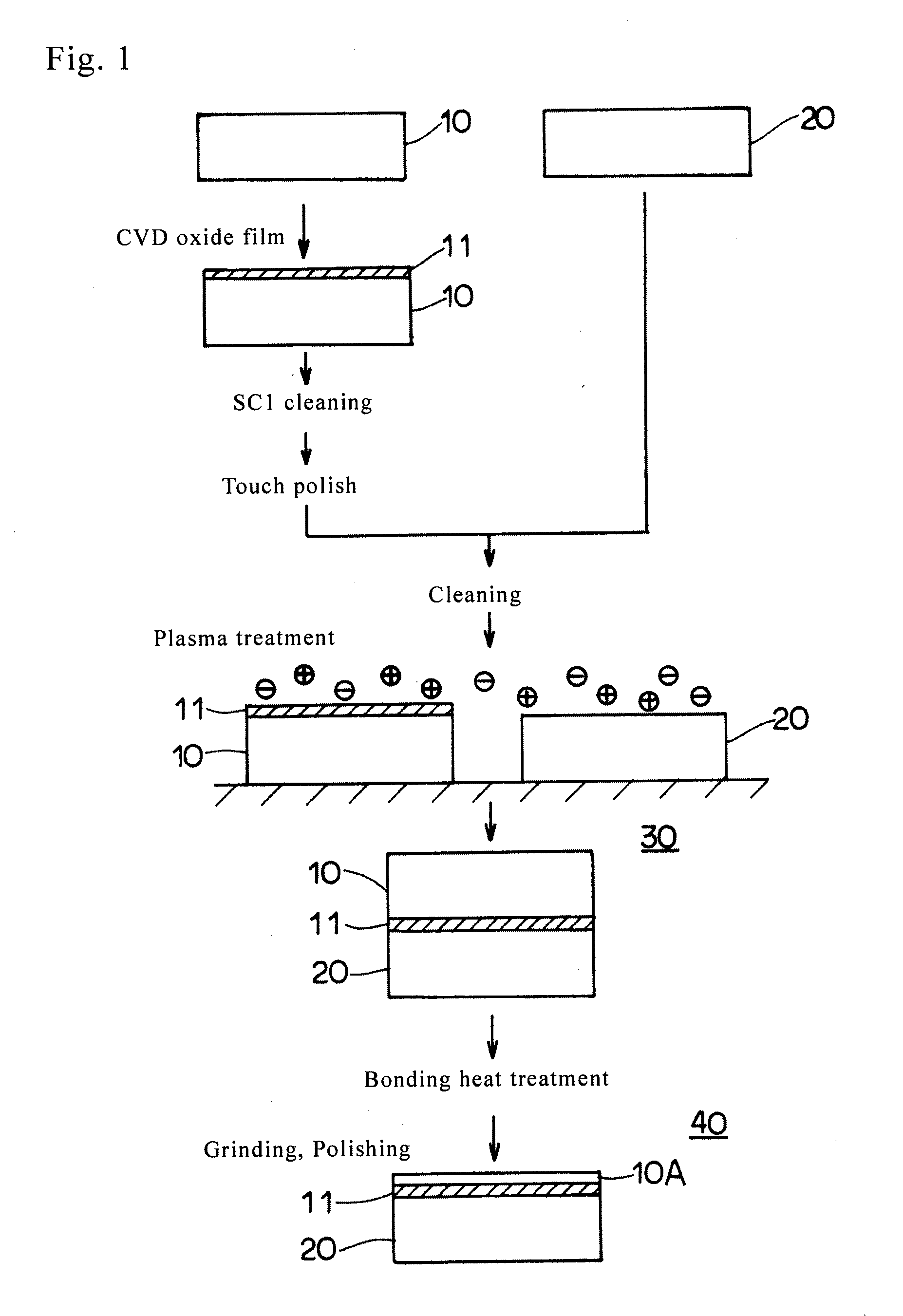
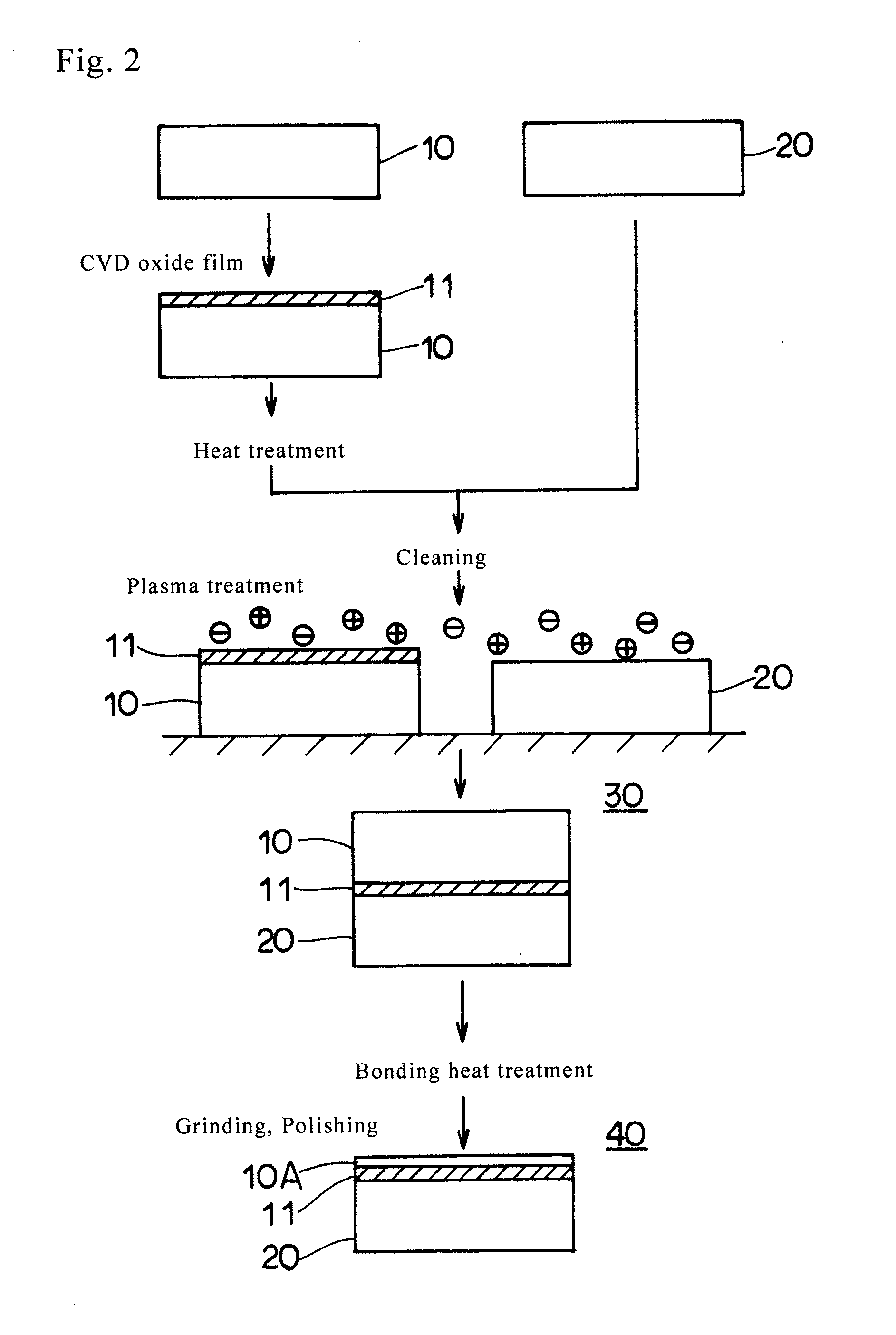
[0035]In the following, with reference to the flowchart of FIG. 1, a manufacturing method of a bonded SOI wafer using a wafer bonding method according to a first embodiment of the present disclosure is explained. As illustrated in the flowchart of FIG. 1, first, a p-type single crystal silicon ingot having a predetermined amount of boron added therein is pulled using a CZ method. After that, the single crystal silicon ingot is subjected to block cutting, slicing, chamfering, mirror polishing, and the like. By doing this, a wafer (first wafer) 10 for an active layer and a wafer (second wafer) 20 for a support substrate are obtained each having a thickness of 725 μm, a diameter of 200 mm, a resistivity of 10-20 Ωcm, being of a p-type, and having one surface mirror-finished. After that, the wafer 10 for an active layer is put into an atmospheric pressure CVD apparatus. A TEOS (tetraethoxysilane) gas is supplied into the furnace. At a heating temperature of 450° C., a CVD oxide film 11 ...
first experimental example
[0051]On the surface of the wafer for an active layer obtained by using the method according to the first embodiment, a CVD oxide film having a thickness of 0.2 μm was formed. After that, the surface of the CVD oxide film was subjected to an SC1 cleaning, and then, the cleaned surface was subjected to a touch polish. As a result, the amount of organic substances attached to the surface of the CVD oxide film was reduced to below 0.01 ng / cm2. Next, this wafer for an active layer and the wafer for a support substrate were bonded at a room temperature, and the void occurrence of the resulting bonded wafer was examined. As a result, no void was detected (void free). Further, with respect to a wafer for an active layer and a wafer for a support substrate of the first experimental example, which were prepared separately from the above, the two bonding interfaces were plasma treated, and the two wafers were bonded to make a bonded wafer. Void occurrence was examined. The result was void fre...
second experimental example
[0052]On the surface of the wafer for an active layer, a CVD oxide film was formed. After that, the wafer for an active layer was subjected to heat treatment. As a result, the amount of organic substances attached to the surface of the CVD oxide film was below 0.01 ng / cm2, the same as in the first experimental example. Next, this wafer for an active layer and the wafer for a support substrate were bonded at a room temperature to make a bonded wafer. Void occurrence in the bonded wafer was examined. As a result, several voids were detected. Further, with respect to a wafer for an active layer and a wafer for a support substrate of the second experimental example, which were prepared separately from the above, the two bonding interfaces were plasma treated. After that, the two wafers were bonded to make a bonded wafer. Void occurrence in the bonded wafer was examined. The result was void free, the same as in the first experimental example (FIG. 6). The rest of the experimental conditi...
PUM
 Abstract
Description
Claims
Application Information