Low-voltage thin-film field-effect transistors

a field-effect transistor and low-voltage thin-film technology, applied in the direction of instruments, electrical equipment, material analysis, etc., can solve the problems of limiting the range of potential applications, high operating voltage of solution-processed tfts incorporating either organic/polymeric or inorganic semiconductors, and the cost of solution-processing of semiconductor and/or gate dielectric layers, etc., to facilitate fabrication of tft, increase the geometrical capacitance of the transistor channel

Inactive Publication Date: 2011-05-19
IMPERIAL INNOVATIONS LTD
View PDF5 Cites 17 Cited by
  • Summary
  • Abstract
  • Description
  • Claims
  • Application Information

AI Technical Summary

Benefits of technology

[0007]The native oxide dielectric layer provides multiple benefits. It is simple to form; a separate deposition step for forming the dielectric is not required, thus facilitating fabrication of the TFT. Moreover, the native oxide layer can function as an ultra-thin gate dielectric layer, thereby increasing the geometrical capacitance of the transistor channel. Since the current flowing through the semiconducting channel is directly proportional to the geometrical capacitance of the channel, this enables the operating voltage, and hence the power consumption of the transistor, to be reduced drastically. A further benefit is that the native oxide layer provides suitable surface chemistry whereby functionalisation with self-assembling monolayer (SAM) materials can be performed. Such SAM dielectric materials can provide extra insulation so that the gate leakage current is minimised.
[0008]The use of spray pyrolysis to form the semiconductor layer renders the TFT solution-processable, thereby facilitating manufacture.
[0014]Preferably the native oxide layer is of the order of 10 nm or less in thickness. This small thickness (compared with conventional TFT dielectrics) dramatically increases the geometrical capacitance of the transistor (e.g. to around 0.4-1 μF / cm2, compared with 15-20 nF / cm2 for a 200 nm thick SiO2 dielectric). This enables the magnitude of the operating voltage of the transistor to be reduced to absolute values below 2 V (i.e. values below |2| V). This is roughly 20-50 times lower than the operating voltages for conventional TFTs. As a result, the power consumption of these devices during operation is also reduced by a similar factor.
[0018]The semiconductor layer may be deposited in a pulsed manner. By providing a time delay between successive sprays, this enables the solution vapours to adsorb to the substrate and convert to the semiconductor material.
[0023]The method may further comprise functionalising the dielectric layer with a self-assembling monolayer dielectric layer. This improves the electrical insulation of the dielectric layer and, in turn, improves the operating characteristics of the TFT.

Problems solved by technology

Unfortunately, the vast majority of solution-processed TFTs incorporating either organic / polymeric or inorganic semiconductors require high operating voltages, typically in the range of tens of volts.
A number of efforts have achieved this strategic goal but typically at the cost of solution-processability of the semiconductor and / or the gate dielectric layers.
Unfortunately, organic TFTs are characterised by relatively low carrier mobilities that limit the range of potential applications.

Method used


Image

  • Low-voltage thin-film field-effect transistors
  • Low-voltage thin-film field-effect transistors
  • Low-voltage thin-film field-effect transistors

Examples


Embodiment Construction

[0056]The present embodiments represent the best ways known to the applicants of putting the invention into practice. However, they are not the only ways in which this can be achieved.

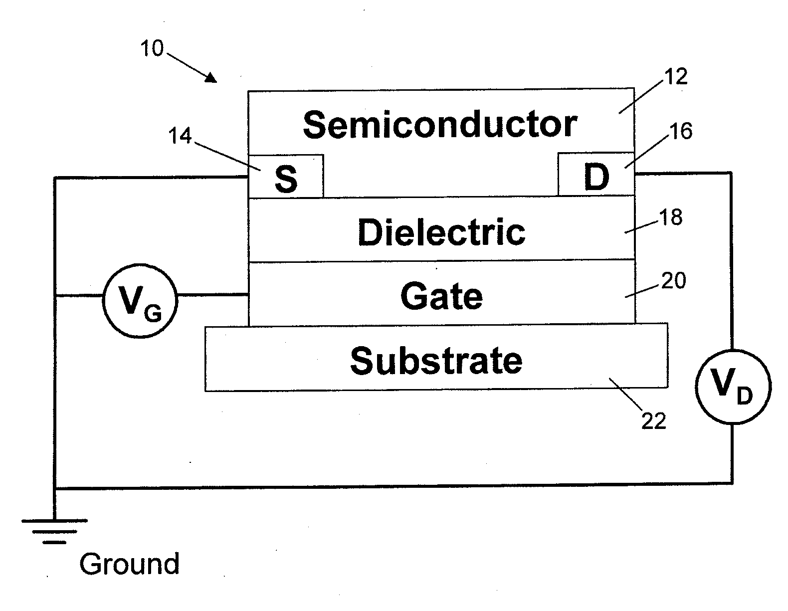
[0057]By way of introduction, as illustrated in FIG. 1, a conventional bottom-gate bottom-contact TFT device 10 consists of a semiconducting active layer 12 applied onto a three-terminal electrode architecture comprising a source electrode 14, a drain electrode 16 and a gate electrode 20. The gate electrode 20 is separated from the semiconductor layer 12 and the source and drain electrodes by a dielectric layer 18.

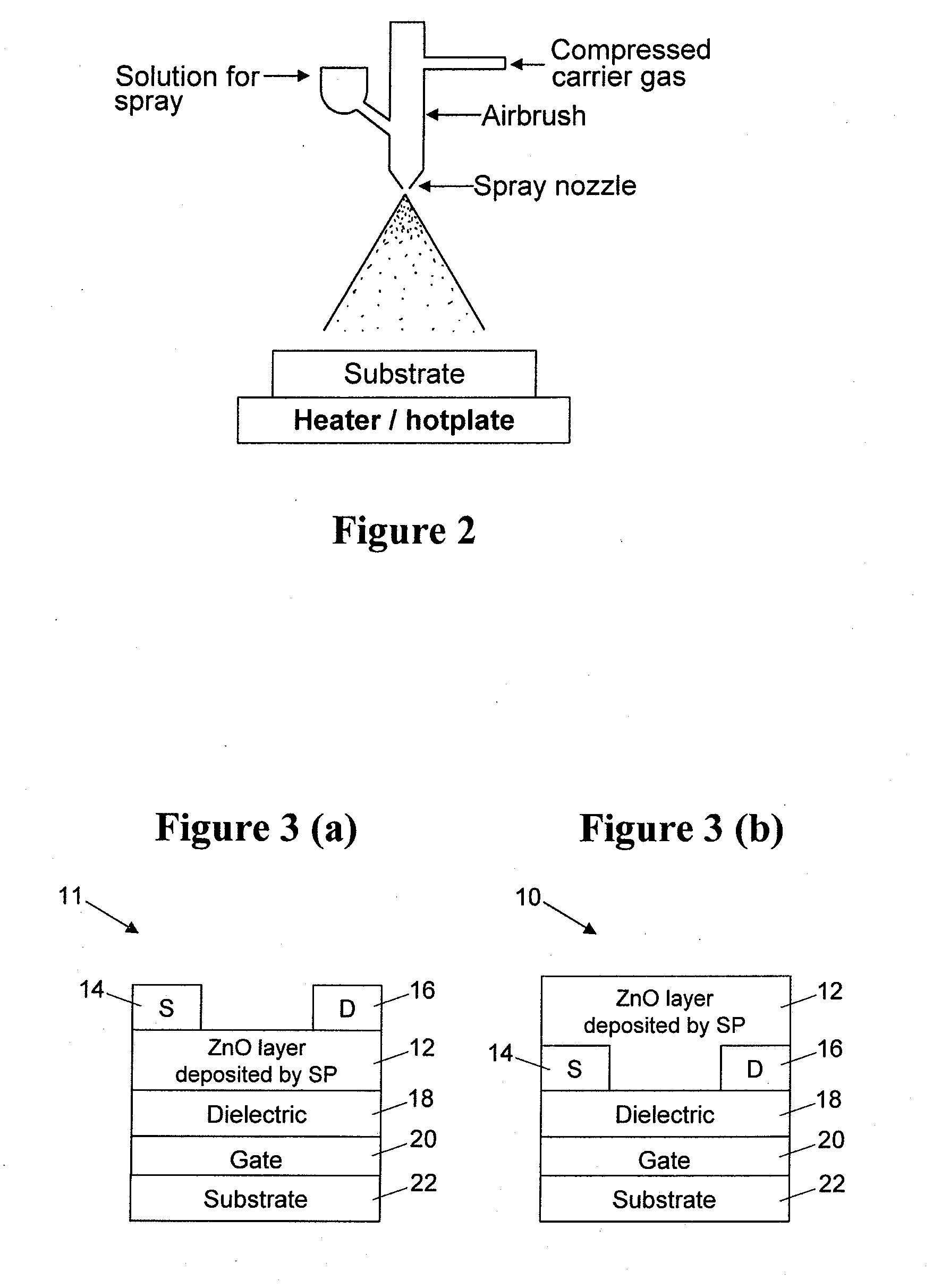
[0058]In embodiments of the present invention, the semiconducting layer 12 is deposited using spray pyrolysis (which may be abbreviated to “SP” herein). This builds upon our earlier work on the spray pyrolysis of semiconducting layers, as described in WO 2008 / 129238 (for a TiO2 semiconducting layer) and, more recently, PCT / GB2009 / 001635 (which claims priority from GB 0811962.0) for other semi...


PUM

PropertyMeasurementUnit
thicknessaaaaaaaaaa
temperatureaaaaaaaaaa

Abstract

A low-voltage thin-film field-effect transistor is formed by forming a gate, forming a dielectric layer on the surface of the gate, forming a source region and a drain region, and forming a semiconductor layer adjacent the dielectric layer. The dielectric layer is formed as a native oxide layer by oxidizing the surface of the gate. The semiconductor layer is deposited by spray pyrolysis. The dielectric layer may be functionalized with a self-assembling monolayer dielectric layer. The dielectric layer may be formed as a self-assembling monolayer, without first forming a native oxide (or other) dielectric layer.

Description

[0001]This invention relates, in part, to thin-film field-effect transistors for low-voltage and low-power applications, and a fabrication method thereof.BACKGROUND TO THE INVENTION[0002]Semiconducting thin-film transistors (TFTs) comprise a substrate, a semiconducting layer, a dielectric layer, and conducting materials for the source, drain and gate electrodes. Depending on the gate potential (VG) and the drain potential (VD), the channel current (i.e. the current flowing from the source electrode to the drain electrode, often referred to as ID) can be modulated.[0003]Advances in solution-processable TFTs are sought for the realisation of high throughput yet low-cost electronic applications. Examples include integrated logic circuits [1] and backplanes for conventional as well as novel, e.g. flexible etc, optical displays [2]. Unfortunately, the vast majority of solution-processed TFTs incorporating either organic / polymeric or inorganic semiconductors require high operating voltage...

Claims


Application Information

Patent Timeline
Patent Type & Authority Applications(United States)
IPC IPC(8): H01L29/786H01L21/336G01N33/00
CPCH01L29/4908H01L29/78681H01L27/1292H01L29/66969H01L29/7869
Inventor ANTHOPOULOS, THOMASBRADLEY, DONAL DONAT CONORBASHIR, ANEEQAWOBKENBERG, PAUL HENRICH
Owner IMPERIAL INNOVATIONS LTD
Why Eureka
Try Eureka