Bonding wire for semiconductor

a technology of semiconductors and bonding wires, applied in the direction of solvents, manufacturing tools, transportation and packaging, etc., can solve the problems of increasing electrical resistance, deteriorating bonding strength, and difficult to comprehensively satisfy the various characteristics requisites of bonding wires, so as to improve the sphericity of a ball and workability of a wire, improve the stability of a compressive bonded shape at a ball bonded part, and improve the effect of pull strength

Active Publication Date: 2011-05-26
NIPPON STEEL CHEMICAL CO LTD +1
View PDF1 Cites 28 Cited by
  • Summary
  • Abstract
  • Description
  • Claims
  • Application Information

AI Technical Summary

Benefits of technology

[0058]According to a bonding wire with a multilayer structure, improvement of both sphericity of a ball and workability of a wire can be accomplished. Moreover, stabilization of a compressive bonded shape at a ball bonded part can be promoted. Furthermore, a successive bonding property after a wire is left in an atmosphere for a long time can be improved. Still further, a pull strength can be improved. Yet further, a...

Problems solved by technology

Conversely, alloying may cause deterioration of a bonding property and increase of an electrical resistance, so that it is difficult to comprehensively satisfy various characteristics requisites for the bonding wires.
Moreover, because gold is expensive, other kinds of metal which have a low material cost are desired, and bonding wires made of copper which have a low material cost and which have a good electrical conductivity are created.
According to the copper bonding wires, however, a bonding strength is deteriorated due to oxidization of a wire surface, and a wire surface is likely to be corroded when encapsulated in a resin.
The silver bonding wires have such advantages that silver i...

Method used


Image

  • Bonding wire for semiconductor
  • Bonding wire for semiconductor

Examples


examples

[0123]Next, an explanation will be given of examples of the present invention.

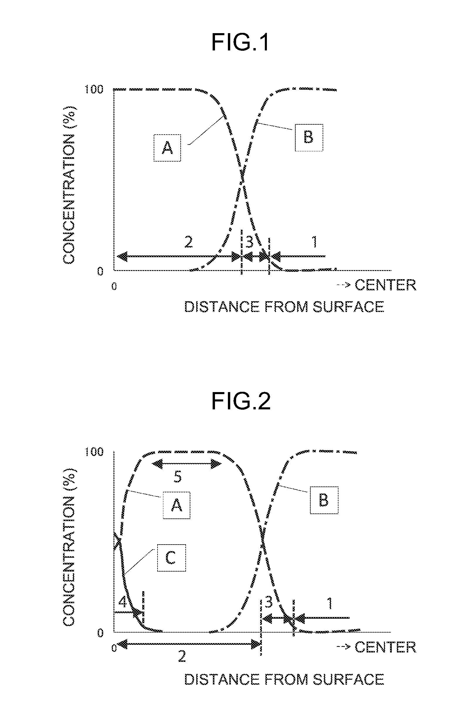
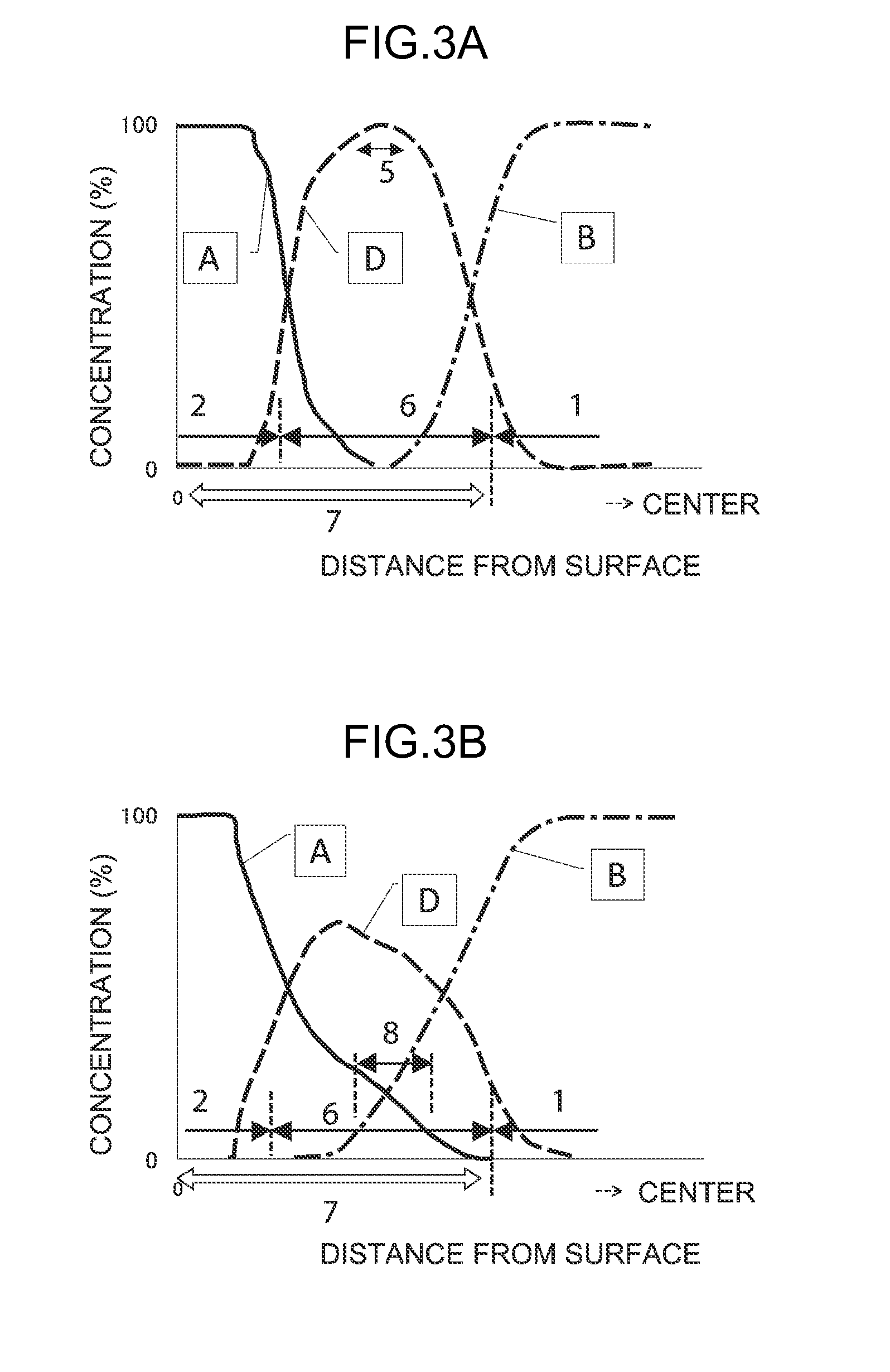
[0124]As raw materials of a bonding wire, Cu, Au or Ag which was a highly pure material having a purity of equal to or larger than about 99.99 mass % was used for a core member, and Pd for an outer layer and Au or Ag which was a material for a surface concentrated layer or an intermediate layer having a purity of equal to or larger than 99.9 mass % were prepared. In a step of melting the core member, an appropriate amount of alloy element was added.

[0125]A thin wire thinned to a certain wire diameter was used as the core member, and the Pd outer layer and the surface concentrated layer or the intermediate layer of at least either one of Au and Ag were formed on the wire surface by electrolytic plating, nonelectrolyte plating, or vapor deposition. A technique of forming the outer layer at a final wire diameter and a technique of forming the outer layer, the surface concentrated layer or the intermediate lay...


PUM

PropertyMeasurementUnit
Temperatureaaaaaaaaaa
Fractionaaaaaaaaaa
Percent by massaaaaaaaaaa

Abstract

It is an object of the present invention to provide a multilayer wire which can accomplish both ball bonding property and wire workability simultaneously, and which enhances a loop stability, a pull strength, and a wedge bonding property. A semiconductor bonding wire comprises a core member mainly composed of equal to or greater than one kind of following elements: Cu, Au, and Ag, and an outer layer formed on the core member and mainly composed of Pd. A total hydrogen concentration contained in a whole wire is within a range from 0.0001 to 0.008 mass %.

Description

TECHNICAL FIELD[0001]The present invention relates to a semiconductor bonding wire used for connecting an electrode on a semiconductor device and a wiring of a circuit wiring board (a lead frame, a substrate, a tape, etc.,) together.BACKGROUND ART[0002]Recently, thin wires each having a wire diameter of 20 to 50 μm or so are popularly used as semiconductor bonding wires (hereinafter, referred to as bonding wires) for connecting an electrode on a semiconductor device and an external terminal together. A thermal compressive bonding technique with the aid of ultrasound is generally applied to bond bonding wires, and a general-purpose bonding device, and a capillary jig which allows a bonding wire to pass through the interior thereof for connection are used. A leading end of a bonding wire is heated and melted by arc heat inputting, a ball is formed by surface tension, and then the ball is compressively bonded on an electrode of a semiconductor device heated within a range from 150 to 3...

Claims


Application Information

Patent Timeline
IPC IPC(8): B23K35/12B23K35/24
CPCH01L2924/01033H01L2924/01045H01L2924/14H01L2924/0105H01L2924/01014H01L2924/01024C22C5/04H01L2924/01006H01L2224/48479H01L2224/48624H01L2224/85464H01L2224/85207H01L2924/01079H01L2224/48011H01L2924/01029H01L2224/85186C22C5/06H01L2224/43848H01L2224/85439C22C5/02H01L2224/43H01L2924/01015H01L2924/01004H01L2224/45015H01L2224/4569B32B15/018H01L2224/48247H01L2924/01013H01L2924/01047H01L2224/45664Y10T428/12222H01L2924/20753H01L2924/01028H01L2924/01078H01L2924/01327H01L2924/01005H01L2924/0103H01L2924/3025H01L24/43C22C9/00H01L2224/85444H01L2224/45686H01L2224/45572H01L2924/01082H01L2224/45565H01L2224/85065H01L24/45H01L2924/20751H01L2924/20752H01L2224/45147H01L2224/48471H01L2924/10253H01L2924/01018C22C21/12H01L2224/85045C22C21/02H01L2224/45139H01L2224/45164H01L2224/43986H01L2224/05624H01L2924/01046H01L2224/85075H01L2924/00015H01L2924/01001H01L2224/45144H01L2924/00014H01L2924/00011H01L2924/20754H01L2924/20105H01L2924/20106H01L2924/20107H01L2924/01202H01L2924/01007H01L2924/01205H01L2224/45644H01L2224/45639H01L2224/45669H01L2224/45655H01L2224/45657H01L2224/45671H01L2224/45666H01L2924/20656H01L2924/20652H01L2924/20645H01L2924/20654H01L2924/20655H01L2924/00H01L2224/48227H01L2224/48824H01L2924/013H01L2224/45169H01L2224/48639H01L2224/48644H01L2224/48664H01L2224/48839H01L2224/48844H01L2224/48864H01L2924/181H01L2924/20108H01L2924/20109H01L2924/2011H01L2924/20111H01L2924/00013H01L2924/01049
Inventor UNO, TOMOHIROTERASHIMA, SHINICHIYAMADA, TAKASHIOISHI, RYOODA, DAIZO
Owner NIPPON STEEL CHEMICAL CO LTD
Why Eureka
Try Eureka