

Semiconductor device
- Summary
- Abstract
- Description
- Claims
- Application Information
AI Technical Summary
Benefits of technology
Problems solved by technology
Method used
Image

Examples
embodiment 1
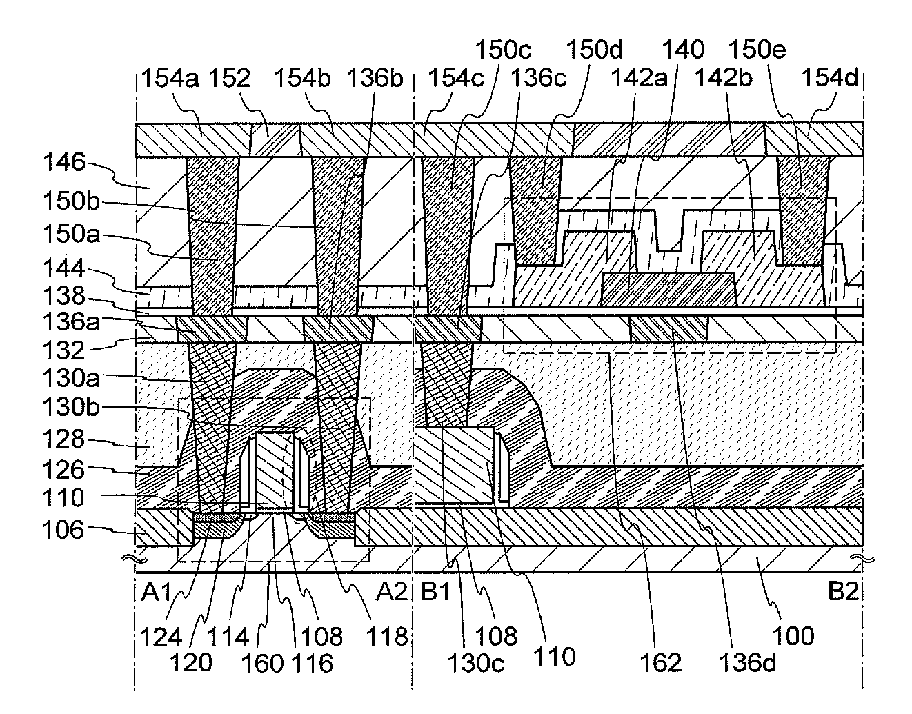
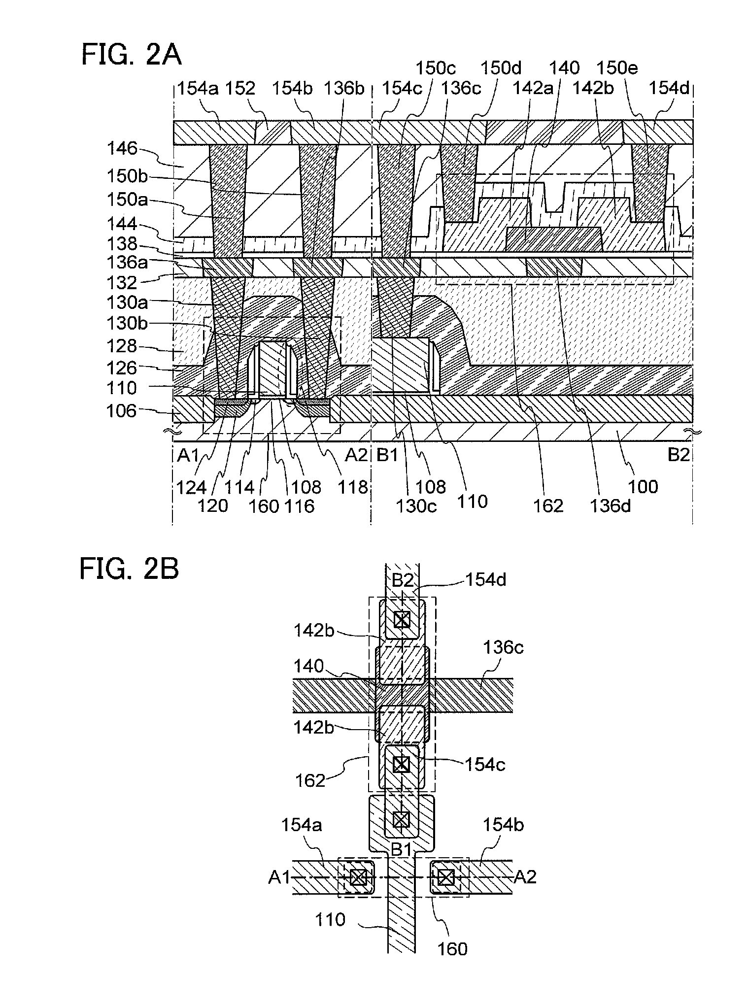
[0056]In this embodiment, structures and manufacturing methods of semiconductor devices according to one embodiment of the disclosed invention are described with reference to FIG. 1, FIGS. 2A and 2B, FIGS. 3A to 3H, FIGS. 4A to 4G, FIGS. 5A to 5D, FIG. 6, FIGS. 7A and 7B, FIGS. 8A and 8B, FIG. 9, FIG. 10, FIG. 11, FIG. 12, FIGS. 13A and 13B, FIGS. 14A and 14B, and FIGS. 15A and 15B.
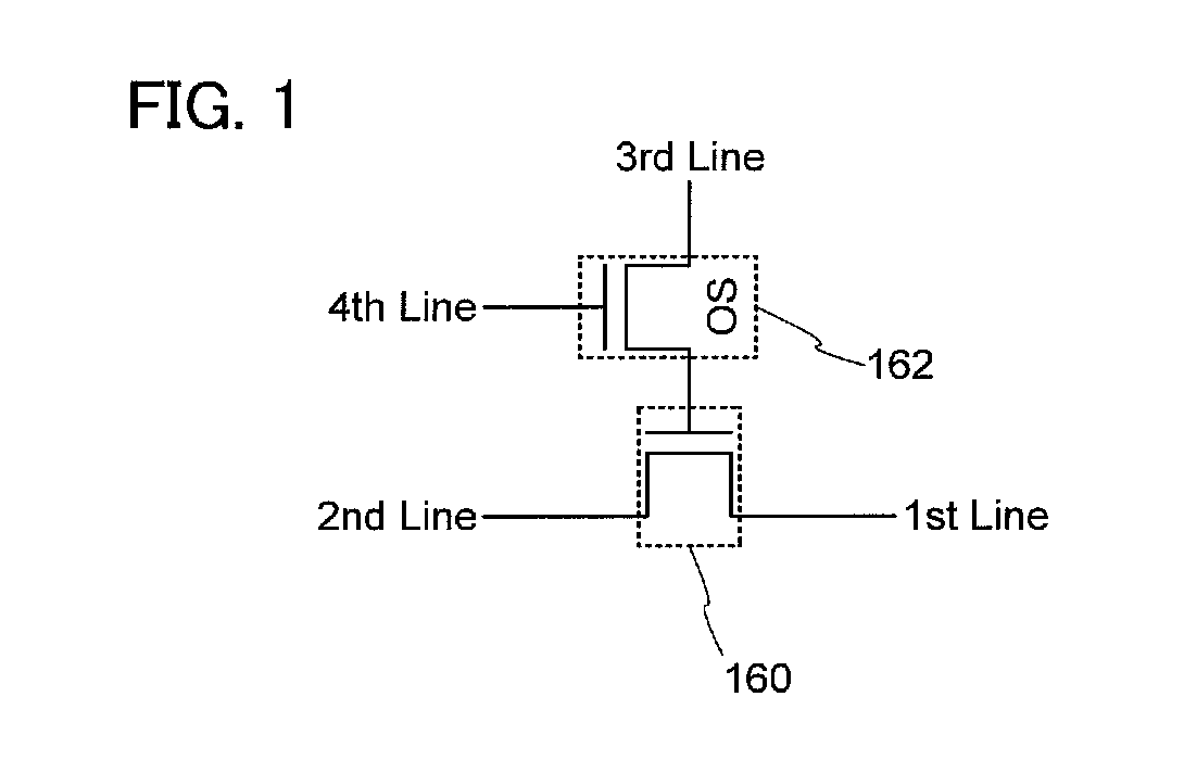
[0057]FIG. 1 illustrates an example of a circuit structure of a semiconductor device.
[0058]The semiconductor device includes a transistor 160 which uses a material other than an oxide semiconductor and a transistor 162 which uses an oxide semiconductor. Note that a mark “OS” is added to the transistor 162 in FIG. 1 to show that the transistor 162 uses an oxide semiconductor (OS). This applies also to other circuit diagrams of other embodiments.
[0059]Here, a gate electrode of the transistor 160 is electrically connected to one of a source electrode and a drain electrode of the transistor 162. A first wirin...
embodiment 2
[0213]In this embodiment, a circuit configuration of a semiconductor device according to one embodiment of the present invention and an operation method thereof will be described.
[0214]FIG. 16 illustrates an example of a circuit diagram of a memory cell included in the semiconductor device. A memory cell 200 illustrated in FIG. 16 includes a first signal line S1, a word line WL, a transistor 201 (a first transistor), a transistor 202 (a second transistor), and a capacitor 203. The transistor 201 is formed using a material other than an oxide semiconductor and the transistor 202 is formed using an oxide semiconductor. Here, the transistor 201 is preferably formed to have a structure similar to that of the transistor 160 in Embodiment 1. In addition, the transistor 202 is preferably formed to have a structure similar to that of the transistor 162 in Embodiment 1. Further, the memory cell 200 is electrically connected to a source line SL and a bit line BL and may be electrically connec...
embodiment 3
[0246]An example of the reading circuit 212 included in a semiconductor device according to one embodiment of the present invention will be described with reference to FIG. 18.
[0247]The reading circuit 212 illustrated in FIG. 18 includes a transistor 204 and a sense amplifier 205. A bias voltage Vbias is applied to a gate electrode of the transistor 204, and a predetermined current flows through the transistor 204. A reference potential Vref is input to one input terminal of the sense amplifier.
[0248]When data is read, the other input terminal of the sense amplifier 205 and a bit line BL connected to a memory cell from which data is read are electrically connected to each other.
[0249]A memory cell has a different resistance corresponding to data “1” or data “0” stored therein. Specifically, when the transistor 201 in a selected memory cell is on, the memory cell has a low resistance; whereas when the transistor 201 in a selected memory cell is off, the memory cell has a high resista...
PUM
 Abstract
Description
Claims
Application Information