Silicon carbide semiconductor device

a silicon carbide and semiconductor technology, applied in the direction of semiconductor devices, basic electric elements, electrical apparatus, etc., can solve the problems of low breakdown field of silicon carbide, inability to achieve insufficiently high withstand voltage in the trench mosfet, and decrease in current density, so as to reduce the area of the body region, reduce the dead space in the on state, and facilitate the effect of channel mobility

Inactive Publication Date: 2011-05-26
NAT INST OF ADVANCED IND SCI & TECH
View PDF3 Cites 34 Cited by
  • Summary
  • Abstract
  • Description
  • Claims
  • Application Information

AI Technical Summary

Benefits of technology

[0020]According to the present invention, the area of the body regions is minimized. Accordingly, the dead space in an ON state is reduced. Also, the trench faces are formed by {11-20} planes having high channel mobility.
[0021]Accordingly, the withstand voltage in the structure of the MOSFET according to the present invention becomes higher than those in conventional cases, and the ON resistance can be lowered.

Problems solved by technology

However, since the breakdown field of silicon carbide is high, a high electric field is applied to each gate insulating film at the bottoms of the trenches in a blocking state, and a sufficiently high withstand voltage cannot be achieved in the trench MOSFET.
This is not desirable, since the forward blocking voltage in this device design is lowered.
However, in a device having a current flowing vertically in the substrate, the p-type region 19 is a dead space, and causes a decrease in current density.
However, the breakdown field of silicon carbide is high.
As a result, a high electric field is applied to the gate insulating film at the bottom of each trench in a blocking state, and a sufficiently high withstand voltage cannot be achieved in a trench MOSFET.

Method used


Image

  • Silicon carbide semiconductor device
  • Silicon carbide semiconductor device
  • Silicon carbide semiconductor device

Examples


Embodiment Construction

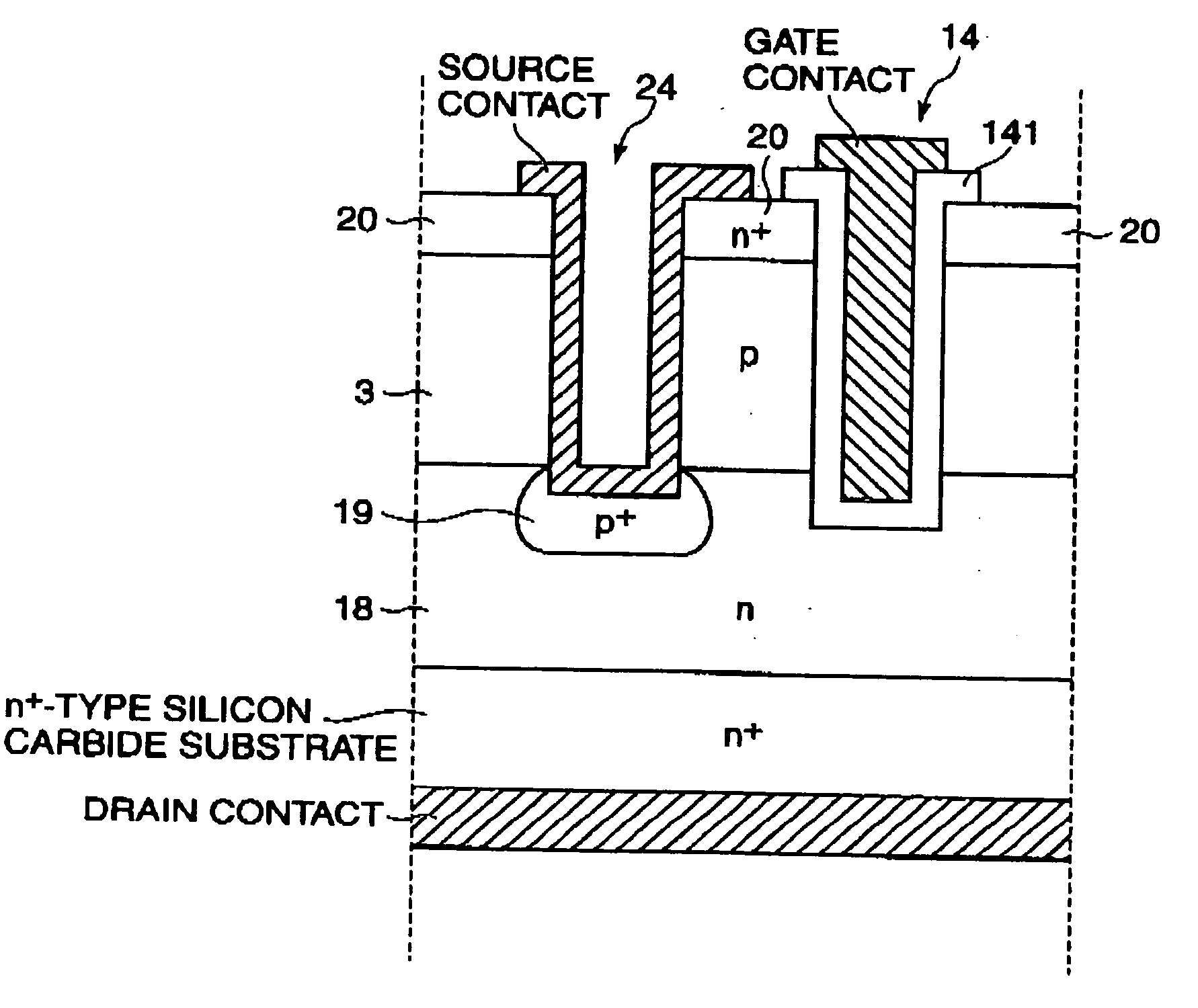
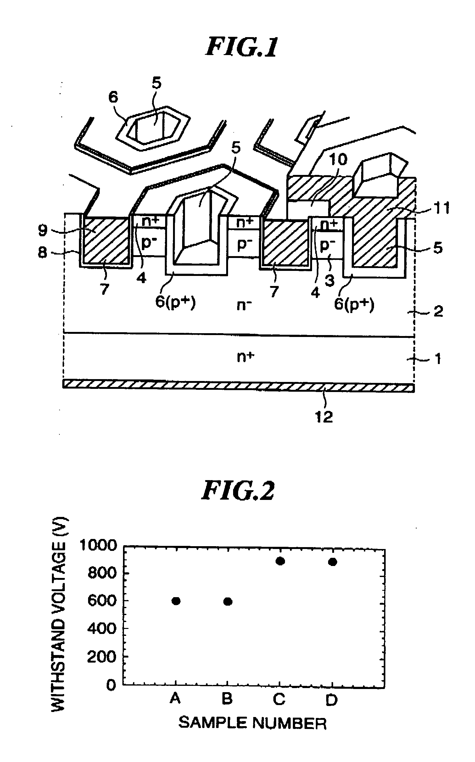
[0028]FIG. 1 shows the structure of a silicon carbide trench MOSFET of the present invention. An n−-type drift layer 2 having thickness of from 5 to 30 μm that is doped with nitrogen of 3×10¹⁵ to 3×1016 cm−3 and made of 4H-SiC is deposited on a low-resistance n+-type substrate 1 that is made of 4H-SiC and has a C-plane as a principal surface. The low-resistance n+-type substrate 1 may be a 4H-SiC substrate that has a principal surface with an orientation inclined from the (000-1) plane to one degree or less.

[0029]Further, p-type base layers 3 having thickness of from 1 to 3 μm that are doped with aluminum of 5×10¹⁶ to 2×1018 cm−3 and made of 4H-SiC are deposited on the type drift layer 2. The p-type base layers 3 may also be formed by an ion implantation technique.

[0030]N+-type source regions 4 doped with phosphorus of approximately 2×1020 cm−3 are formed on the surfaces of the p-type base layers 3, and first trench grooves 5 that reach the n−-type drift layer 2 are formed in the ce...


PUM


Abstract

The area of each body region is minimized, and the gate oxide films at the bottoms of the trenches are more effectively protected by depletion layers extending from the body regions.
According to the present invention, an n-type drift layer and a p-type base region are stacked on an n+-type silicon carbide substrate, and an n+-type source region is formed in a predetermined region of a surface portion in the base region. A gate trench is formed in a trench groove that reaches the drift layer. A p-type body region is formed at a deeper location than the gate trench. The p-type body region is adjacent to the gate trench but is not in contact with the gate trench. When viewed from above, the gate trench having a hexagonal shape surrounds the p-type body region. The side faces of the gate trench are formed only by {11-20} planes of silicon carbide.

Description

BACKGROUND OF THE INVENTION[0001]1. Field of the Invention[0002]The present invention relates to a silicon carbide semiconductor device that has a power-converting semiconductor switching device with a lower ON resistance and a higher withstand voltage with the use of a silicon carbide substrate.[0003]2. Description of the Related Art[0004]As a power-converting semiconductor switching device using a silicon carbide substrate, a trench MOSFET is an effective structure to lower ON-resistance, having smaller unit cell structures and a higher current density than a planar MOSFET. However, since the breakdown field of silicon carbide is high, a high electric field is applied to each gate insulating film at the bottoms of the trenches in a blocking state, and a sufficiently high withstand voltage cannot be achieved in the trench MOSFET.[0005]FIG. 5 illustrates the structure of an n-channel vertical insulating-gate field-effect transistor (a vertical power MOSFET) disclosed in Japanese Pat...

Claims


Application Information

Patent Timeline
Patent Type & Authority Applications(United States)
IPC IPC(8): H01L29/161
CPCH01L29/045H01L29/0696H01L29/1608H01L29/7813H01L29/41766H01L29/4238H01L29/66068H01L29/41741
Inventor HARADA, SHINSUKE
Owner NAT INST OF ADVANCED IND SCI & TECH
Why Eureka
Try Eureka