Start signal detector circuit

a detector circuit and start signal technology, applied in the direction of electrical control, pulse technique, instruments, etc., can solve the problems of circuit oscillation and significant increase in input capacitance, and achieve the effect of improving the rectification efficiency of the rectifier circuit for detection, stably detecting a start signal, and reducing power consumption of the smart plate system

Active Publication Date: 2011-05-26
NEC CORP
View PDF2 Cites 7 Cited by
  • Summary
  • Abstract
  • Description
  • Claims
  • Application Information

AI Technical Summary

Benefits of technology

[0025]According to the start signal detector circuit of the present invention, input signals at phases opposite to each other are applied to a control terminal and a second terminal of a non-linear three-terminal element, specifically, a gate and a source of a MOSFET (or a base and an emitter of a bipolar transistor). In this way, the non-linearity of the non-linear three-terminal element can be...

Problems solved by technology

For amplifying such an infinitesimal voltage to approximately 1 V which can be utilized as a start signal, an amplifier having a gain of approximately 100 dB is required at a later stage, resulting in a concern that an excessively high gain will cause the circuit to oscilla...

Method used


Image

  • Start signal detector circuit
  • Start signal detector circuit
  • Start signal detector circuit

Examples


first exemplary embodiment

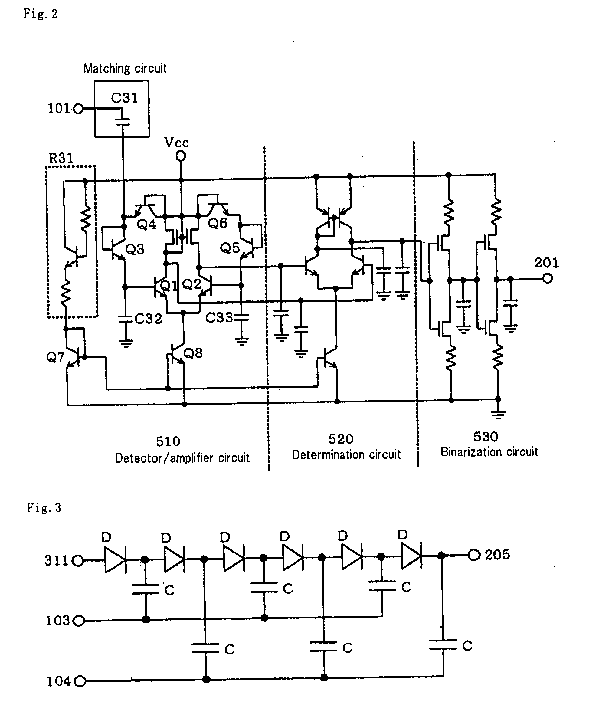
[0058]FIG. 6 is a circuit diagram of a start signal detector circuit of a first exemplary embodiment of the present invention, In FIG. 6, 101 designates an RF input terminal; 201 designates an output terminal; 301, 302 designate DC bias terminals; M1, M2 designate MOS transistors; C1, C2 designate capacitors; and R1 designates a resistor. MOS transistor M1 has a drain terminal connected to DC bias terminal 301, and a source terminal connected to RF input terminal 101 through capacitor C1. A DC potential at a gate terminal is supplied from DC bias terminal 302 through resistor R1. Also, MOS transistor M2 has a drain terminal and a gate terminal commonly connected to node N1 and applied with RF signal through capacitor C1. MOS transistor M2 has a source connected to output terminal 201. Also, capacitor C2 for signal charge accumulation is connected to the source of MOS transistor M2.

[0059]In this circuit, a current flows into capacitor C1 from bias terminal 301 through MOS transistor ...

second exemplary embodiment

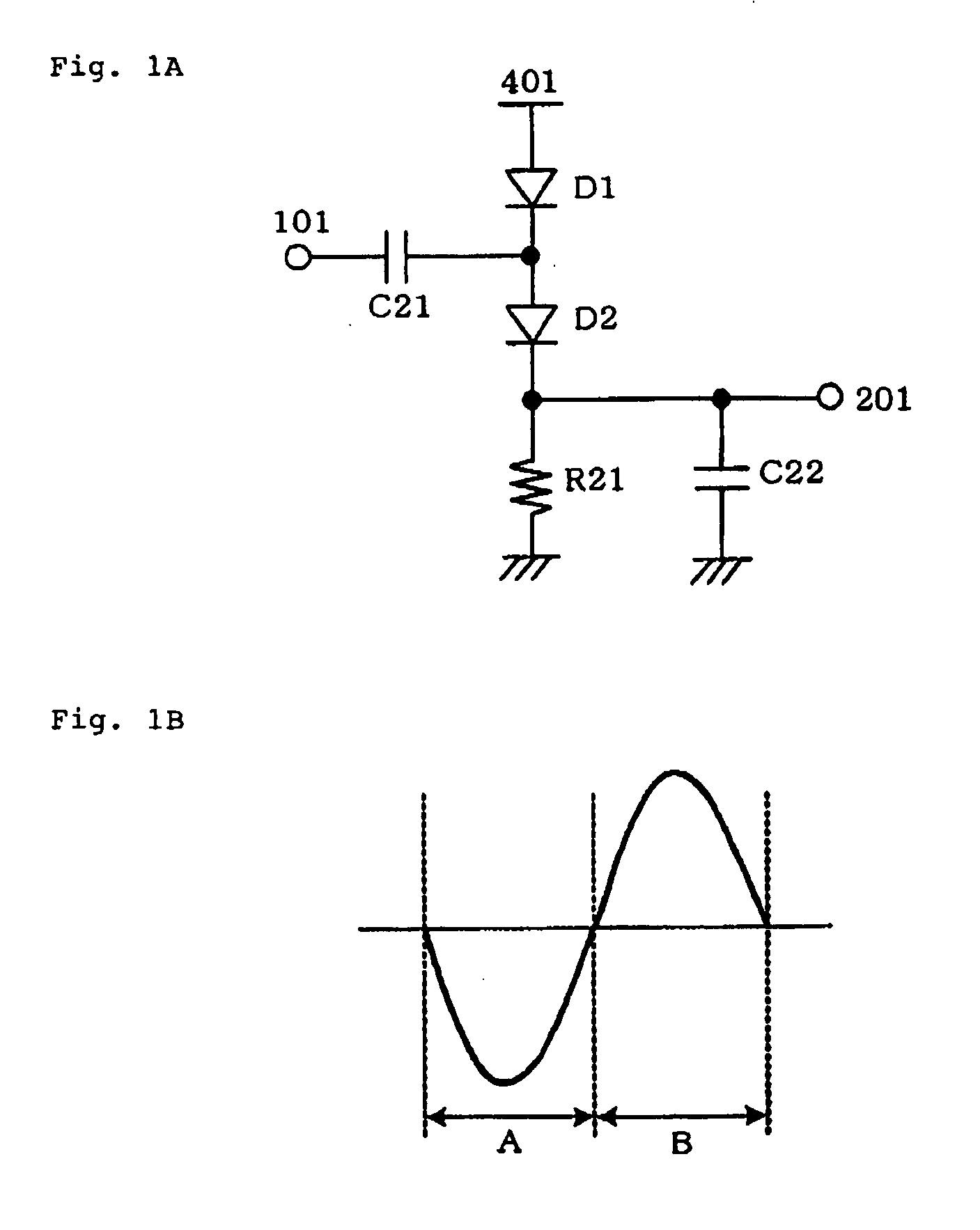
[0060]FIG. 7 is a circuit diagram of a start signal detector circuit of a second exemplary embodiment of the present invention. In FIG. 7, 101 designates an RF input terminal; 102 designates an RF input terminal which is applied with an RF signal at a phase opposite to 101; 201 designates an output terminal; 301, 302 designate DC bias terminals; M1 , M2 designate MOS transistors; C1-C3 designate capacitors; and R1 designates a resistor. MOS transistor M1 has a drain terminal connected to DC bias terminal 301, and a source terminal and a gate terminal connected to RF input terminals 101, 102, respectively, through capacitor C1, C3. Therefore, the source terminal and gate terminal are applied with RF signals at phases opposite to each other. Also, MOS transistor M2 has a drain terminal and a gate terminal commonly connected to node N1 and applied with an RF signal through capacitor C1. MOS transistor M2 has a source connected to output terminal 201, and capacitor C2 for signal charge ...

third exemplary embodiment

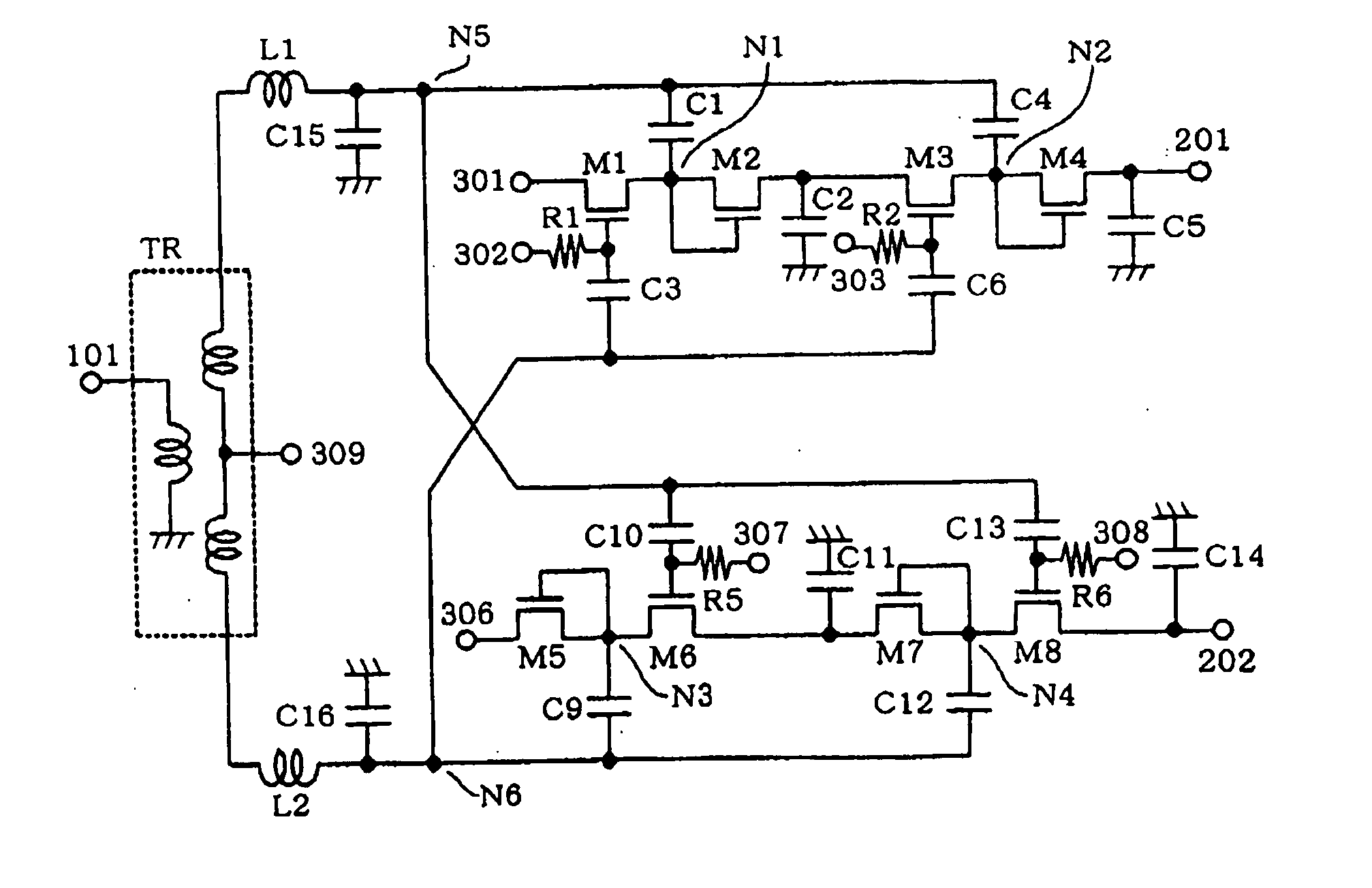
[0062]FIG. 8 is a circuit diagram of a start signal detector circuit of a third exemplary embodiment of the present invention. The circuit of this embodiment comprises series resonance circuits which are added to RF input terminals 101, 102 in the start signal detector circuit of the second exemplary embodiment shown in FIG. 7. Specifically, inductor L1 and capacitor C15 connected to RF input terminal 101 are designed to resonate in series in a desired frequency band, and likewise, inductor L2 and capacitor C16 connected to RF input terminal 102 are designed to resonate in series in a desired frequency band. In this circuit, an impedance viewed from RF input terminals 101, 102 toward the inductor is minimized in the desired frequency band, whereas impedance viewed from nodes N5, N6 toward the inductor is maximized, and the amplitudes of signals at nodes N5, N6 are increased by the resonance, so that the non-linearity of MOS transistor M1 can be further increased. As a result, the re...


PUM


Abstract

The nonlinearity effect of a rectifying element is enhanced, and further a resonant circuit is used to enlarge the input amplitude. Furthermore, the rectifying efficiency of a detection rectifier circuit is enhanced, thereby allowing the gain of an amplifier circuit in the following stage to be set to a low value. Signals having mutually opposite phases are inputted to RF input terminals (101,102). The signal at the terminal (102) is then inputted to the gate of a transistor (M1) via a capacitor (C3), while the signal at the terminal (101) is then inputted, via a capacitor (C1), to a node (N1) to which the source of the transistor (M1) and the gate and drain of a transistor (M2) are connected, whereby a capacitor (C2) is charged with a half-wave voltage-doubled rectified current. DC biases are inputted to terminals (301,302). There are formed series resonant circuits (L1,C15;L2,C16). A plurality of half-wave voltage-doubled rectifier circuits (M1,M2,C1-C3,R1) are connected in cascade.

Description

TECHNICAL FIELD[0001]The present invention relates to a start signal detector circuit, and more particularly, to a circuit which receives radio frequency signal power (RF) at a particular frequency to generate a DC potential (DC) required to intermittently operate an electronic system.BACKGROUND ART[0002]In recent years, DSRC (Dedicated Short Range Communication), which has been studied for development, is a communication system directed to narrow ranges for use in communications between cars on roads such as ETC (Electronic Toll Collection System), a commercial car management system and the like. The DSRC is classified into a light-based system and a radiowave-based system, and is generally deemed to be available for communications in a range of several meters to several hundred meters. The specifications of this system are established by ARIB STD (Association of Radio Industries Businesses standard)—T55 Standard and STD-T75 Standard, and employs a carrier frequency in a range of 5...

Claims


Application Information

Patent Timeline
IPC IPC(8): H03K5/153H03K3/01G05F1/10
CPCF02D2041/0012H03D1/18H03D1/10F02D2200/0812
Inventor MAEDA, TADASHIYAMASE, TOMOYUKI
Owner NEC CORP
Why Eureka
Try Eureka