Soi substrate and manufacturing method thereof

Inactive Publication Date: 2011-05-26
SEMICON ENERGY LAB CO LTD
View PDF18 Cites 4 Cited by
  • Summary
  • Abstract
  • Description
  • Claims
  • Application Information

AI Technical Summary

Benefits of technology

[0022]According to one embodiment of the disclosed invention, a region where gas is trapped is formed in part (the periphery) of the surface to be bonded. Accordingly, an SOI substrate having a semiconductor layer of which surface roughness is suppressed can be provided.

Problems solved by technology

Bubbles tend to become large as the temperature at which the single crystal silicon thin film is separated becomes high, and surface roughness of the single crystal silicon thin film i

Method used


Image

  • Soi substrate and manufacturing method thereof
  • Soi substrate and manufacturing method thereof
  • Soi substrate and manufacturing method thereof

Examples


embodiment 1

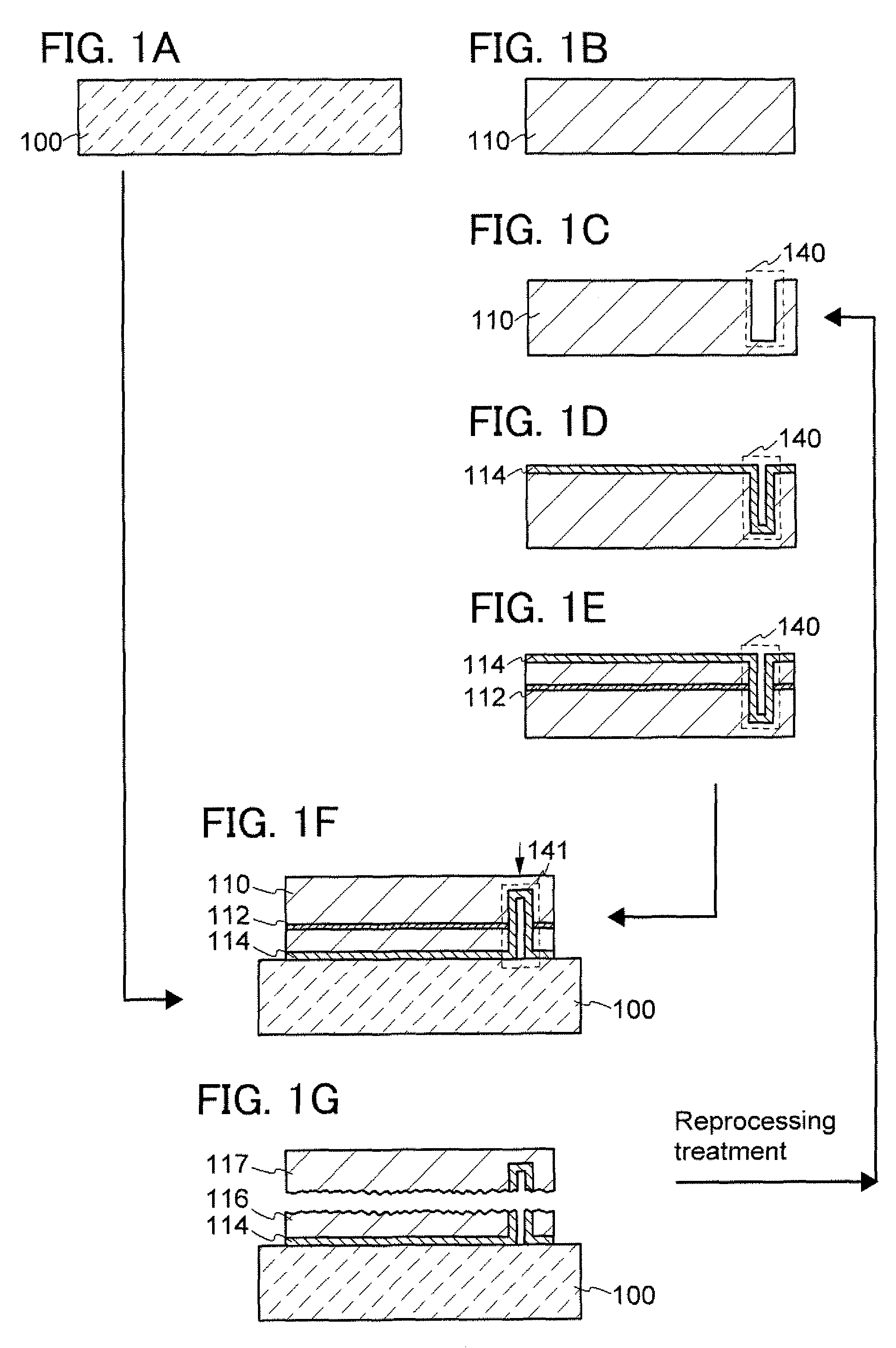
[0040]In this embodiment, an example of a method for manufacturing an SOI substrate will be described with reference to drawings. Specifically, the case of manufacturing an SOI substrate in which a single crystal semiconductor layer is provided over a base substrate will be described.

[0041]First, a base substrate 100 and a semiconductor substrate are prepared (see FIGS. 1A and 1B). In this embodiment, the case where a single crystal semiconductor substrate 110 is used as the semiconductor substrate is described.

[0042]FIG. 1A illustrates the base substrate 100. As the base substrate 100, a substrate formed of an insulator can be used. Specific examples thereof are as follows: a variety of glass substrates used in the electronics industry, such as substrates of aluminosilicate glass, aluminoborosilicate glass, and barium borosilicate glass; a quartz substrate; a ceramic substrate; and a sapphire substrate. Note that when the above-mentioned glass substrate contains a larger amount of ...

embodiment 2

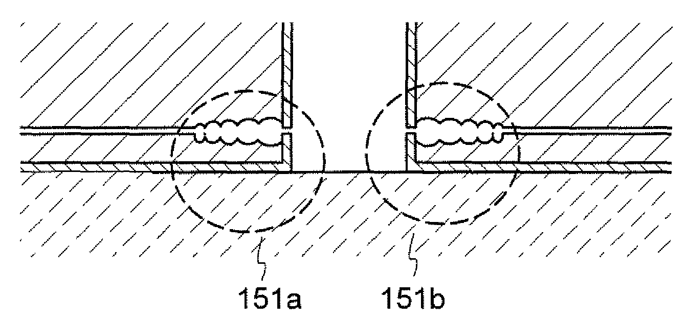
[0104]In this embodiment, the case where reprocessing treatment is performed on the single crystal semiconductor substrate 117 illustrated in FIG. 1G or FIG. 4G will be described with reference to FIGS. 7A to 7C.

[0105]As illustrated in FIG. 7A, a projected portion 126 is formed in the periphery of the single crystal semiconductor substrate 117 after the step in FIG. 1G or FIG. 4G. The projected portion 126 includes a remaining embrittled region 127, a remaining single crystal semiconductor layer 125, and the remaining insulating layer 114, without being bonded to the base substrate 100. In addition, the single crystal semiconductor substrate 117 includes a remaining embrittled region 129.

[0106]The reprocessing treatment of the semiconductor substrate includes at least two etching treatments: an etching treatment for removing the insulating layer 114 (hereinafter, referred to as a first etching treatment) and an etching treatment for removing the remaining single crystal semiconducto...

embodiment 3

[0123]In this embodiment, another example of a method for manufacturing an SOI substrate will be described with reference to drawings.

[0124]First, the base substrate 100 and the single crystal semiconductor substrate 110 as a bond substrate are prepared (see FIGS. 8A and 8C).

[0125]Next, a nitrogen-containing layer 102 (for example, a layer including an insulating film containing nitrogen, such as a silicon nitride (SiNx) film or a silicon nitride oxide (SiNxOy (x>y)) film) is formed over the surface of the base substrate 100 (see FIG. 8B).

[0126]The nitrogen-containing layer 102 formed in this embodiment functions as a layer (a bonding layer) for bonding a single crystal semiconductor layer in a later step. The nitrogen-containing layer 102 also functions as a barrier layer for preventing an impurity contained in the base substrate, such as sodium (Na), from diffusing into the single crystal semiconductor layer.

[0127]As mentioned above, the nitrogen-containing layer 102 is used as a ...


PUM


Abstract

The semiconductor substrate provided with a groove portion is irradiated with ions so that an embrittled region is formed in the semiconductor substrate, the semiconductor substrate and a base substrate are bonded to each other with an insulating layer interposed therebetween and a space which is surrounded by the groove portion in the semiconductor substrate and the base substrate is formed, and heat treatment is performed to separate the semiconductor substrate at the embrittled region, so that the semiconductor layer is formed over the base substrate with the insulating layer interposed therebetween.

Description

BACKGROUND OF THE INVENTION[0001]1. Field of the Invention[0002]The present invention relates to a method for manufacturing a silicon-on-insulator (SOI) substrate, the SOI substrate, and a method for manufacturing a semiconductor device using the SOI substrate.[0003]2. Description of the Related Art[0004]In recent years, instead of a bulk silicon wafer, the use of a silicon-on-insulator (SOI) substrate where a thin single crystal semiconductor layer is provided over an insulating surface has been considered. Because parasitic capacitance generated by a drain of a transistor and a substrate can be reduced by use of an SOI substrate, SOI substrates are attracting attention as substrates which improve performance of semiconductor integrated circuits.[0005]One of known methods for manufacturing SOI substrates is a Smart Cut (registered trademark) method (for example, see Patent Document 1). A summary of a method for manufacturing an SOI substrate by a Smart Cut method is described below...

Claims


Application Information

Patent Timeline
IPC IPC(8): H01L21/30
CPCH01L21/02032H01L21/84H01L21/76254H01L21/30604
Inventor TOKUNAGA, HAJIMEOKUNO, NAOKI
Owner SEMICON ENERGY LAB CO LTD
Why Eureka
Try Eureka