

Material including graphene and an inorganic material and method of manufacturing the material
- Summary
- Abstract
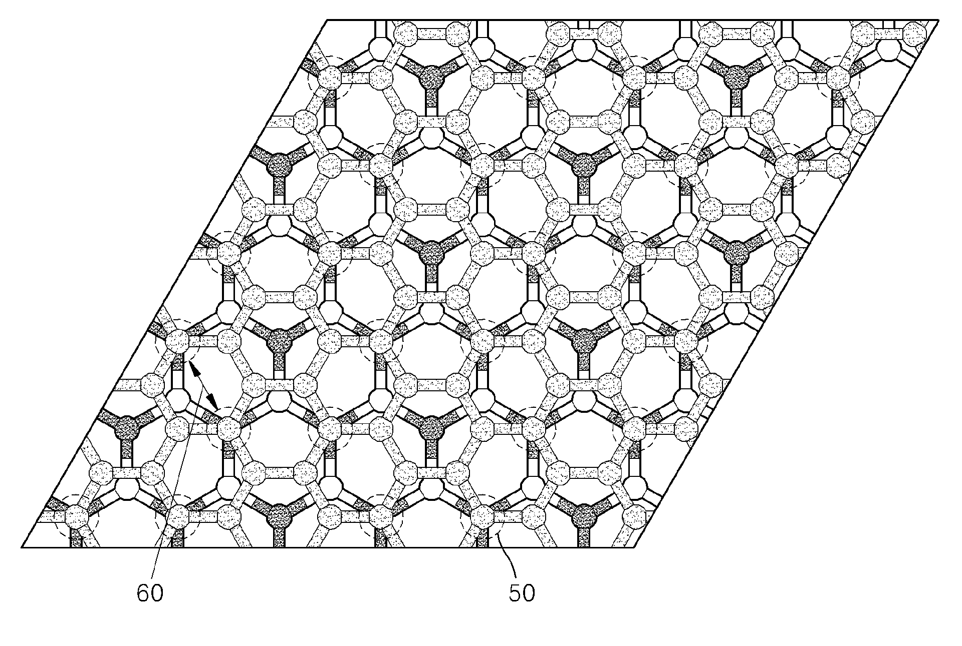
- Description
- Claims
- Application Information
AI Technical Summary
Benefits of technology
Problems solved by technology
Method used
Image

Examples
example 1
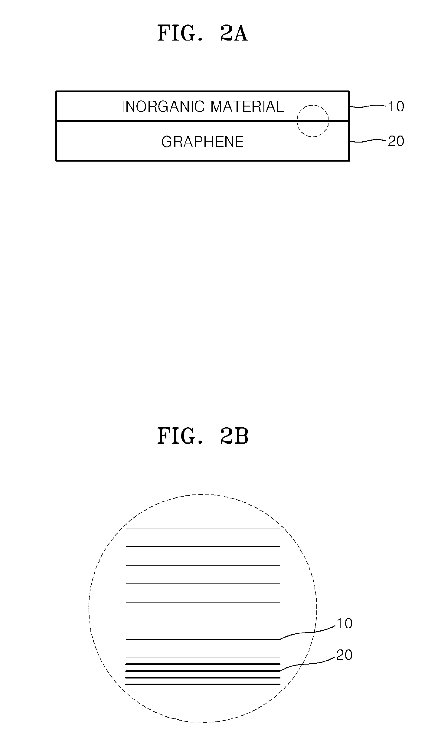
[0072]Zinc acetate powder having the formula (C2H3O2)2Zn was dissolved in ethanol to prepare a 0.01 M solution. Then, the prepared 0.01 M solution was spin-coated or dip-coated on a graphene coated polyethylene terephthalate (“PET”) plastic substrate having the dimensions 2 cm×2 cm, thereby forming a ZnO seed layer. The plastic substrate coated with graphene, on which the ZnO seed layer was formed, was immersed in a solution for growing ZnO in order to grow a ZnO nanorod. The ZnO growth solution was prepared by dissolving zinc nitrate having the formula Zn(NO3)2.6H2O and hexamethylenetetramine (“HMT”) having the formula C6H12N4 in 250 milliliters (ml) of deionized (“DI”) water. The prepared ZnO growth solution had a concentration of 0.025 M Zn nitrate, 0.025 M HMT and DI Water. The plastic substrate, having the ZnO seed layer, was immersed in each of the prepared ZnO growth solutions and then the temperature was increased to 95° C. and held for 3 hours, thereby synthesizing the ZnO ...
example 2
[0075]A ZnO nanorod was grown on a PET substrate coated with indium tin oxide (“ITO”) in the same manner as in Example 1. The ITO layer had a thickness of about 100 nm. The grown ZnO nanorod had the same length and diameter as the ZnO nanorod grown on the graphene coated PET substrate of Example 1. The ITO-coated PET substrate had a sheet resistance of about 70 ohms per square (ohm / sq), and the graphene-coated PET substrate had a sheet resistance of about 200 ohm / sq. A nanoscale power generator (i.e., piezoelectric generator) was manufactured using the substrate in the following manner. A sample formed by growing a ZnO nanorod on the ITO-coated PET substrate was used as a bottom plate and the ITO-coated PET substrate was used as a top plate. The top and bottom plates were coupled to each other to manufacture the nanoscale power generator, and an electrode was connected to the ITO of each of the top and bottom plates, respectively, to measure a current flowing through the nanoscale p...
PUM
 Abstract
Description
Claims
Application Information