Semiconductor device and manufacturing method thereof

Active Publication Date: 2011-06-09
SEMICON ENERGY LAB CO LTD
View PDF100 Cites 38 Cited by
  • Summary
  • Abstract
  • Description
  • Claims
  • Application Information

AI Technical Summary

Benefits of technology

[0036]On-state current and field-effect mobility of the transistor can be improved. Further, off-state current is reduced and on-state current is increased, so that on/off ra

Problems solved by technology

However, there has been a limit to the transistor manufactured using an oxide semiconductor when being used as a switchin

Method used


Image

  • Semiconductor device and manufacturing method thereof
  • Semiconductor device and manufacturing method thereof
  • Semiconductor device and manufacturing method thereof

Examples


embodiment 1

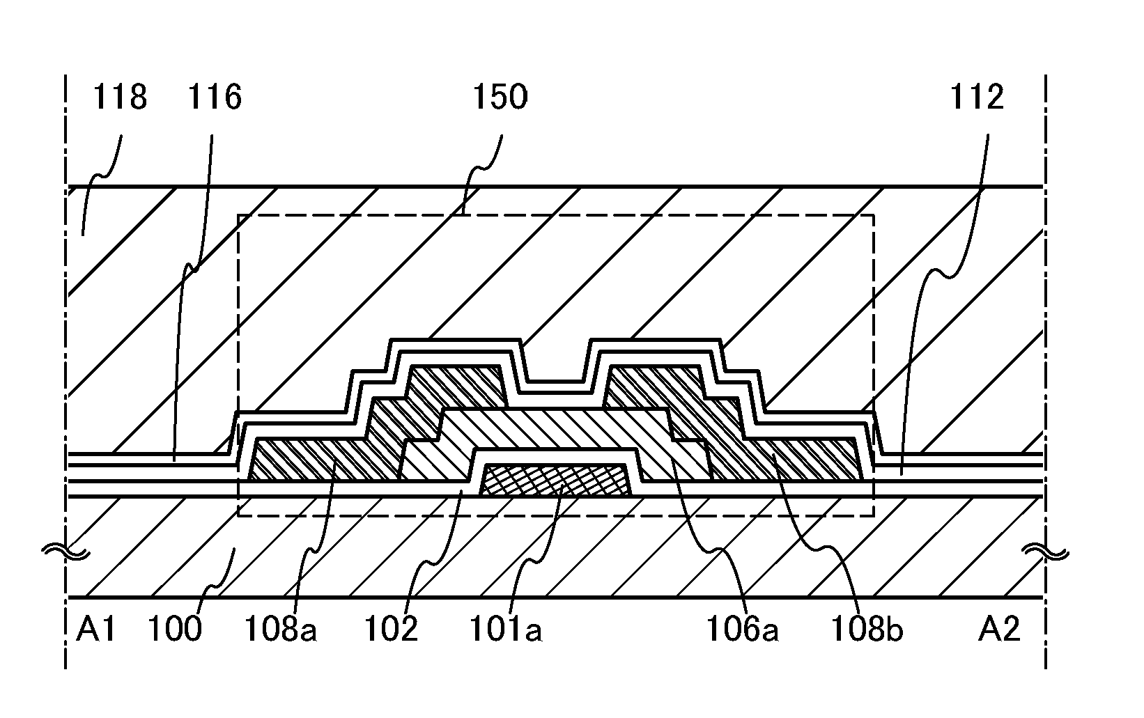
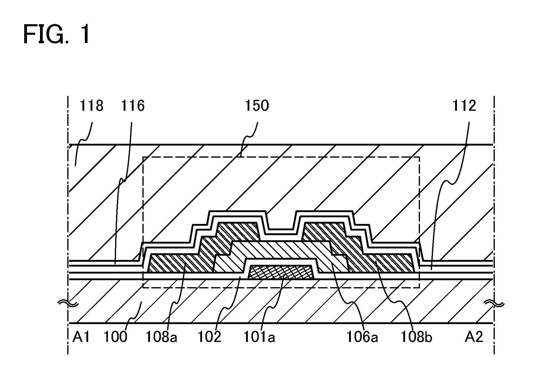
[0052]In this embodiment, a structure of a transistor included in a semiconductor device, which is an embodiment of the present invention, will be described. As the transistor, an inverted staggered transistor will be described in this embodiment.

[0053]In a transistor 150 illustrated in FIG. 1, a gate electrode layer 101a is formed over a substrate 100, and a gate insulating layer 102 is formed over the gate electrode layer 101a. An oxide semiconductor layer 106a, as a channel formation region, is formed over the gate insulating layer 102, and a source or drain electrode layer 108a and a source or drain electrode layer 108b are formed over the oxide semiconductor layer 106a. An insulating layer 112 including oxygen is formed over the source or drain electrode layer 108a, the source or drain electrode layer 108b, and the oxide semiconductor layer 106a. The insulating layer 112 including oxygen is in contact with a back channel of the oxide semiconductor layer 106a. An insulating laye...

embodiment 2

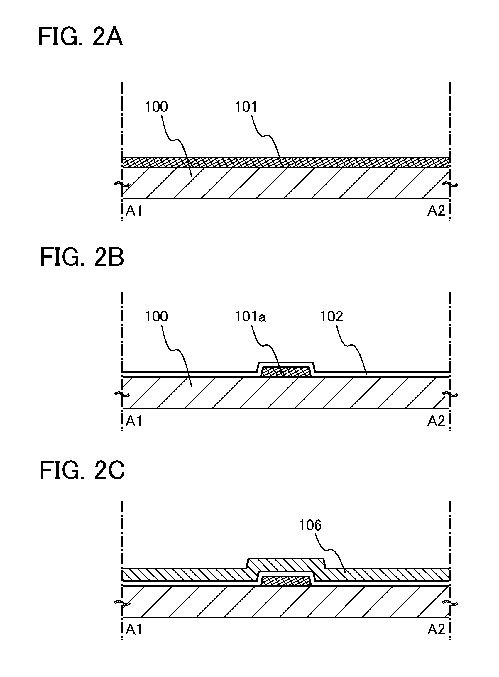
[0074]Next, a manufacturing method of the transistor 150, which is an example of the structure of a semiconductor device, will be described with reference to FIGS. 2A to 2C, FIGS. 3A to 3C, and FIGS. 4A to 4C.

[0075]First, a conductive layer 101 is formed over a substrate 100 (see FIG. 2A).

[0076]Any substrate can be used for the substrate 100 as long as it is a substrate having an insulating surface, and a glass substrate can be used, for example. Further, it is preferable that the glass substrate be a non-alkali glass substrate. As a material of the non-alkali glass substrate, a glass material such as aluminosilicate glass, aluminoborosilicate glass, barium borosilicate glass, or the like is used, for example. Alternatively, as the substrate 100, an insulating substrate formed using an insulator such as a ceramic substrate, a quartz substrate, or a sapphire substrate, a semiconductor substrate which is formed using a semiconductor material such as silicon and whose surface is covere...

embodiment 3

[0145]In this embodiment, another structure and another manufacturing method of the semiconductor device of the above embodiment will be described. In this embodiment, a top-gate transistor will be described.

[0146]First, the transistor 150 which is an example of the structure of a semiconductor device of this embodiment will be described. In the transistor 150 illustrated in FIG. 6D, the oxide semiconductor layer 106a is formed over the substrate 100, and the source and drain electrode layers 108a and 108b are formed over the oxide semiconductor layer 106a. The insulating layer 112 including oxygen is formed so as to cover the source and drain electrode layers 108a and 108b and the oxide semiconductor layer 106a. The insulating layer 112 functions as a gate insulating layer. The insulating layer 112 including oxygen is in contact with a channel of the oxide semiconductor layer 106a. In addition, a gate electrode layer 114 is formed over the insulating layer 112 so as to overlap with...


PUM


Abstract

A manufacturing method of a semiconductor device, which includes the steps of forming a gate electrode layer over a substrate having an insulating surface, forming a gate insulating layer over the gate electrode layer, forming an oxide semiconductor layer over the gate insulating layer, forming a source electrode layer and a drain electrode layer over the oxide semiconductor layer, forming an insulating layer including oxygen over the oxide semiconductor layer, the source electrode layer, and the drain electrode layer, and after formation of an insulating layer including hydrogen over the insulating layer including oxygen, performing heat treatment so that hydrogen in the insulating layer including hydrogen is supplied to at least the oxide semiconductor layer.

Description

TECHNICAL FIELD[0001]The present invention relates to a semiconductor device which includes a circuit including at least a semiconductor element such as a transistor as an element, and a manufacturing method thereof. For example, the present invention relates to an electronic device in which a power device mounted in a power circuit; a semiconductor integrated circuit including a memory, a thyristor, a converter, an image sensor, or the like; an electro-optical device typified by a liquid crystal display panel; or a light-emitting display device including an organic light-emitting element is included as a part.[0002]In this specification, a semiconductor device means any device which can function by utilizing semiconductor characteristics, and an electro-optical device, a semiconductor circuit, and an electronic device are all semiconductor devices.BACKGROUND ART[0003]Transistors formed over a glass substrate or the like have been manufactured using amorphous silicon, polycrystallin...

Claims


Application Information

Patent Timeline
IPC IPC(8): H01L29/12H01L21/336H05B44/00
CPCH01L21/3003H01L29/66969H01L29/7869H01L27/1225H01L21/385H01L29/66742H01L29/78606H01L21/324
Inventor YAMAZAKI, SHUNPEI
Owner SEMICON ENERGY LAB CO LTD
Why Eureka
Try Eureka