Solar Cell Having Quantum Dot Nanowire Array and the Fabrication Method Thereof

a nanowire array and solar cell technology, applied in the field of solar cell quantum dot nanowire array, can solve the problems of low efficiency, low market share of solar cells, and high manufacturing cost of solar cells, and achieve the effects of high efficiency, high efficiency, and enhanced light absorption

Inactive Publication Date: 2011-06-23
KOREA RES INST OF STANDARDS & SCI
View PDF2 Cites 26 Cited by
  • Summary
  • Abstract
  • Description
  • Claims
  • Application Information

AI Technical Summary

Benefits of technology

[0027]The solar cell according to the present invention includes quantum dot nanowire array with a heterostructure including matrix and semiconductor quantum dots, and p-type and n-type semiconductor and electrodes each contacting the quantum dot nanowires. With the solar cell according to the present invention, the band gap energy of the semiconductor quantum dot can be easily controlled, the semiconductor quantum dots having different sizes are provided in the quantum dot nanowire so that the photoelectric conversion can be taken place in a wide spectrum from visible rays to infrared rays, the quantum dots are embedded in the high density quantum dot nanowire arrays so that light absorption can be maximized, and the quantum dot nanowire contact p-type and n-type semiconductor over a large area, conduction efficiency of electrons and holes can be improved. The fabrication method according to the present invention forms a stacked thin film in which matrix layers and semiconductor layers having the thickness of several nanometers and then etches the stacked thin film, thereby fabricating quantum dot nanowire array formed with semiconductor quantum dots.
[0028]Therefore, with the fabrication method according to the present invention, a high efficiency solar cell can be fabricated through a simple and economical process, the wavelength of the absorbing light can be easily controlled by controlling the thickness of the semiconductor layer of the stacked thin film, the sort of matrix, and the contracted diameter of the quantum dot nanowire, etc., and a pair of electron / hole can be generated by absorbing light in a wide spectral region from infrared rays to visible rays.

Problems solved by technology

An n-p diode of inorganic semiconductor material such as silicon or gallium arsenide (GaAs), whose stability and efficiency have been proved, has been mainly used, however, a high manufacturing cost thereof has been an obstacle in substantial utilization of a solar cell.
Although cheaper solar cells using dye-sensitized material and organic / polymeric material have been actively developed, the market share of them is very low to around 3% compared to the silicon based solar cells due to a very low efficiency and a short life span by deterioration.

Method used


Image

  • Solar Cell Having Quantum Dot Nanowire Array and the Fabrication Method Thereof
  • Solar Cell Having Quantum Dot Nanowire Array and the Fabrication Method Thereof
  • Solar Cell Having Quantum Dot Nanowire Array and the Fabrication Method Thereof

Examples


Embodiment Construction

[0036]

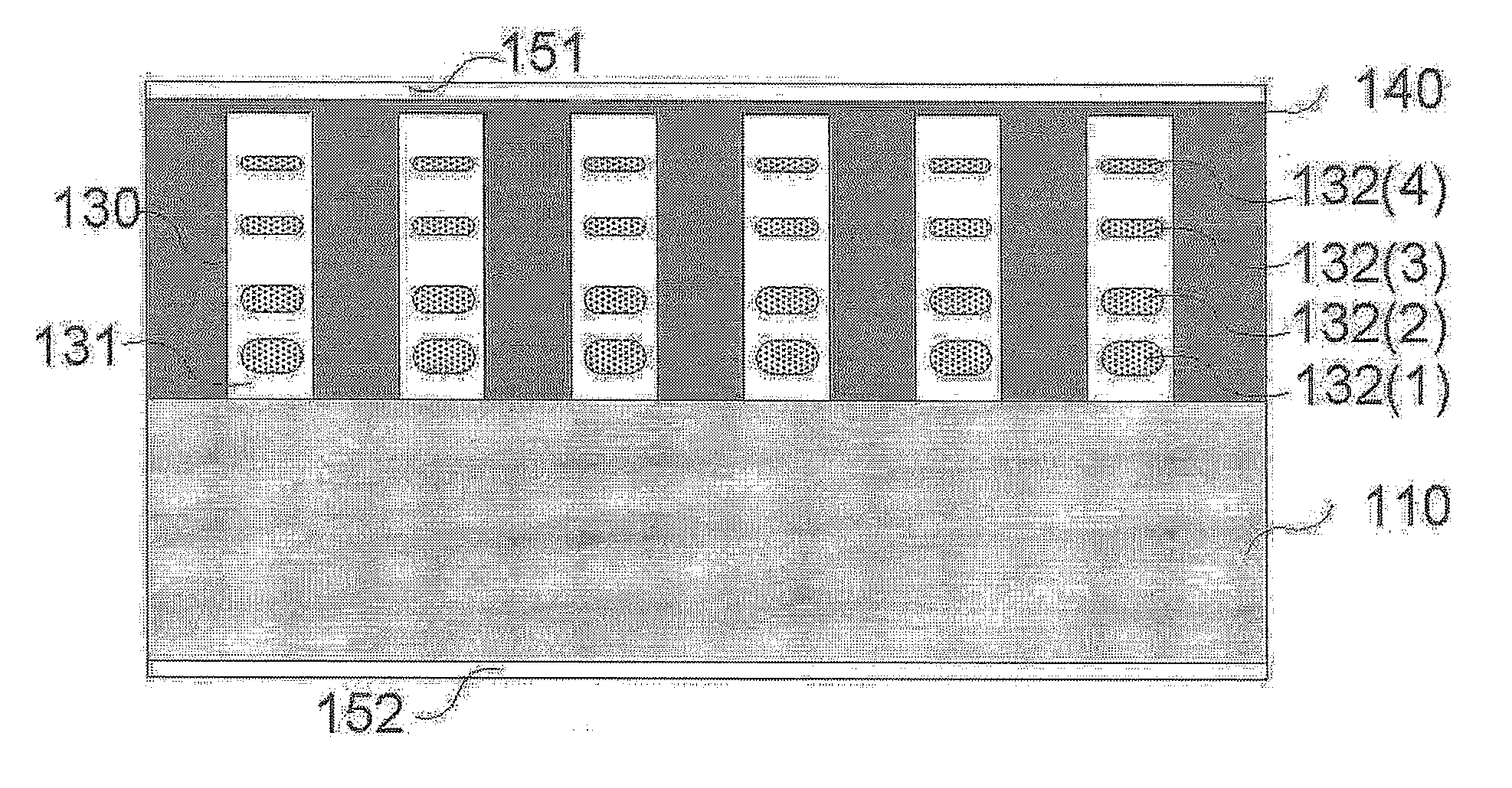
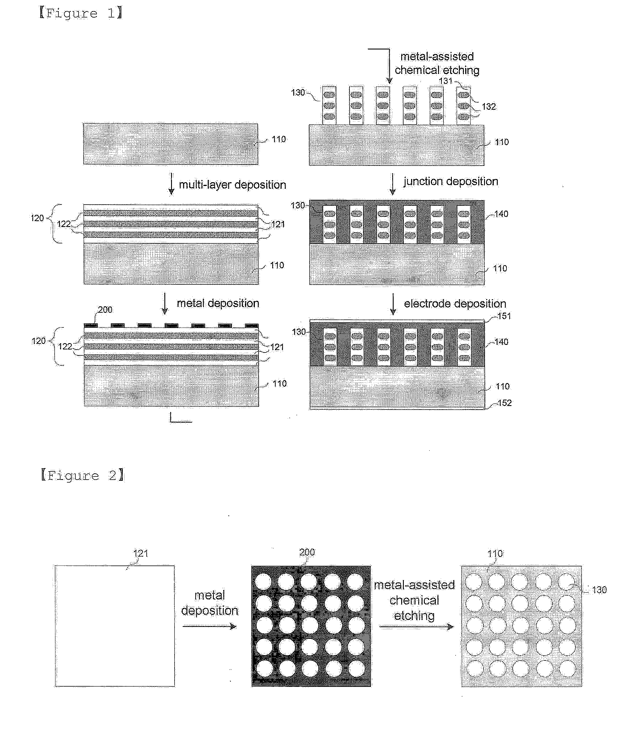
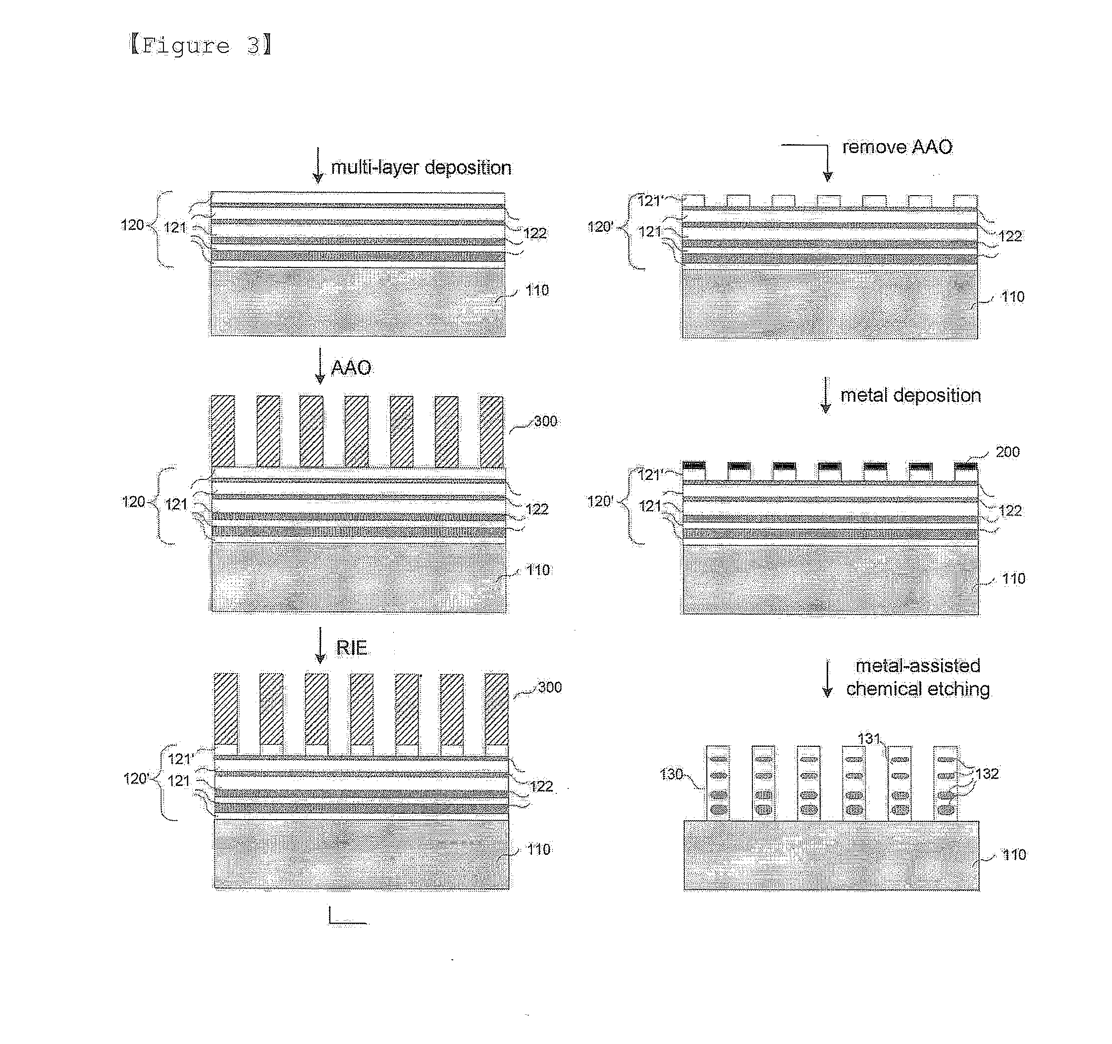
110: p-type semiconductor120: multilayer121: matrix layer122: semiconductor layer120′: multilayer with surface unevenness130: quantum dot nanowire131: matrix132: semiconductor quantum dot140: n-type semiconductor151, 152: electrodes200: metal mesh210: circular metal dot300: nanoporous anodic alumina

BEST MODEL

[0037]Hereinafter, a solar cell having quantum dot nanowire array and the fabrication method thereof according to the present invention will be described in detail with reference to the accompanying drawings. The drawings set forth herein are provided so that those skilled in the art can fully understand the present invention. Therefore, the present invention may be embodied in different forms and should not be construed as limited to the embodiments set forth herein. Like reference numerals refer to like elements throughout.

[0038]At this time, if there are no specific definitions in technical and scientific terminologies used herein, the terminologies have meanings that a...


PUM

PropertyMeasurementUnit
thicknessaaaaaaaaaa
diameteraaaaaaaaaa
thicknessaaaaaaaaaa

Abstract

The present invention relates to a solar cell having quantum dot nanowire array and the fabrication method thereof. The solar cell according to the present invention includes quantum dot nanowire array with a heterostructure including matrix and semiconductor quantum dots, and p-type and n-type semiconductor and electrodes each contacting the quantum dot nanowires. With the solar cell according to the present invention, the band gap energy of the semiconductor quantum dot can be easily controlled, the semiconductor quantum dots having different sizes are provided in the quantum dot nanowire so that the photoelectric conversion can be performed in the wide spectrum from visible rays to infrared rays, the quantum dot is embedded in the high density quantum dot nanowire array so that light absorption can be maximized, and the quantum dot nanowire contact p-type and n-type semiconductor over a wide area, conduction efficiency of electrons and holes can be improved.

Description

TECHNICAL FIELD[0001]The present invention relates to a solar cell having quantum dot nanowire array and the fabricating method thereof, and more particularly to a solar cell having quantum dot nanowire array in which semiconductor quantum dots are internally embedded, and the fabrication method thereof.BACKGROUND ART[0002]Since the Kyoto protocol aiming at resulting carbon dioxide (CO2) emission, which are thought to contribute the global warming, had been adopted as of December, 1997, studies on renewable and clean alternative energy sources such as solar energy, wind power, and water power, have been actively developed in order to reduce a great quantity of carbon dioxide (CO2).[0003]A photovoltaic device (solar cell), which is spotlighted as clean alternative energy, means a device to generate current-voltage using photovoltaic effects that a semiconductor absorbs light to generate electrons and holes.[0004]An n-p diode of inorganic semiconductor material such as silicon or gall...

Claims


Application Information

Patent Timeline
Patent Type & Authority Applications(United States)
IPC IPC(8): H01L31/0352H01L31/18
CPCH01L27/1446H01L31/028Y02E10/547H01L31/1804H01L31/035272Y02P70/50B82Y40/00H01L31/042H01L31/18
Inventor KIM, KYUNG JOONGLEE, WOO
Owner KOREA RES INST OF STANDARDS & SCI
Why Eureka
Try Eureka