Derivatized fullerene-based dopants for organic semiconductors

a technology of organic semiconductors and dopants, which is applied in the direction of sustainable manufacturing/processing, non-metal conductor manufacturing, and final product manufacturing, etc., can solve the problems of high process control and regulation costs, inability to always be sufficiently precise, and large manufacturing process in large technical production plants

Active Publication Date: 2011-06-30
TECHNION RES & DEV FOUND LTD
View PDF6 Cites 18 Cited by
  • Summary
  • Abstract
  • Description
  • Claims
  • Application Information

AI Technical Summary

Benefits of technology

[0054]As used herein the term “method” refers to manners, means, techniques and procedures for accomplishing a given task including, but not limited to, those manners, means, techniques and procedures either known to, or readily developed from known manners, means, techniques and procedures by practitioners of the chemical, pharmacological, biological, biochemical and medical arts.
[0055]Unless otherwise defined, all technical and / or scientific terms used herein have the same meaning as commonly understood by one of ordinary skill in the art to which the invention pertains. Although methods and materials similar or equivalent to those described herein can be used in the practice or testing of embodiments of the invention, exemplary methods and / or materials are described below. In case of conflict, the patent specification, including definitions, will control. In addition, the materials, methods, and examples are illustrative only and are not intended to be necessarily limiting.

Problems solved by technology

The compounds previously investigated have disadvantages for technical use in the production of doped semiconductor organic layers or of suitable electronic components with doped layers of this kind, since the manufacturing processes in large technical production plants, or those on a technical scale, cannot always be sufficiently precisely controlled.
This leads to high control and regulation expense within the process in order to obtain the desired product quality, or to undesirable tolerances of the products.
In addition, there are disadvantages in the use of previously known organic donors with regard to electronic component structures such as light-emitting diodes (OLEDs), field-effect transistors (FETs) or solar cells themselves, since the said production difficulties in the handling of dopants may result in undesirable heterogeneities in the electronic components or undesirable aging effects of the electronic components.

Method used


Image

  • Derivatized fullerene-based dopants for organic semiconductors
  • Derivatized fullerene-based dopants for organic semiconductors
  • Derivatized fullerene-based dopants for organic semiconductors

Examples


example 1

Potentiodynamic Electrochemical Measurements of Doped Systems

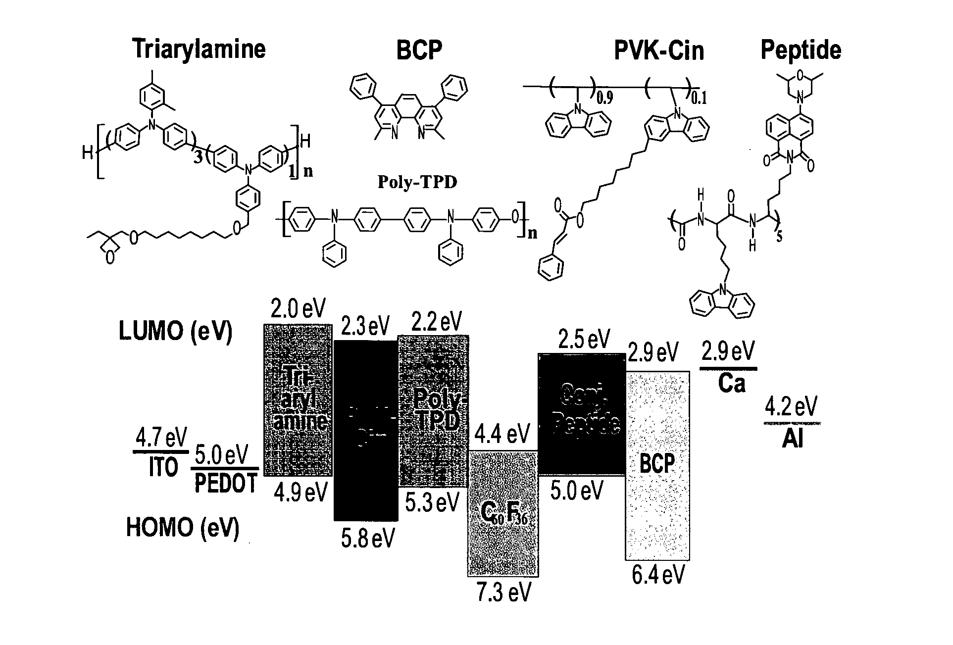
[0185]To characterize the ability and capacity for doping of C60F36, its HOMO-LUMO gap was measured and compared to other C60 derivatives.

[0186]The OSC polymer, poly(3-hexylthiophene-2,5-diyl) (P3HT, CAS N. 104934-50-1) was selected as an exemplary OSC polymer to show the doping effect of the C60 and an exemplary fullerene derivative [6,6]-phenyl-C61-butyric acid methyl ester (PCBM), which is commonly used in the art as an excited state acceptor.

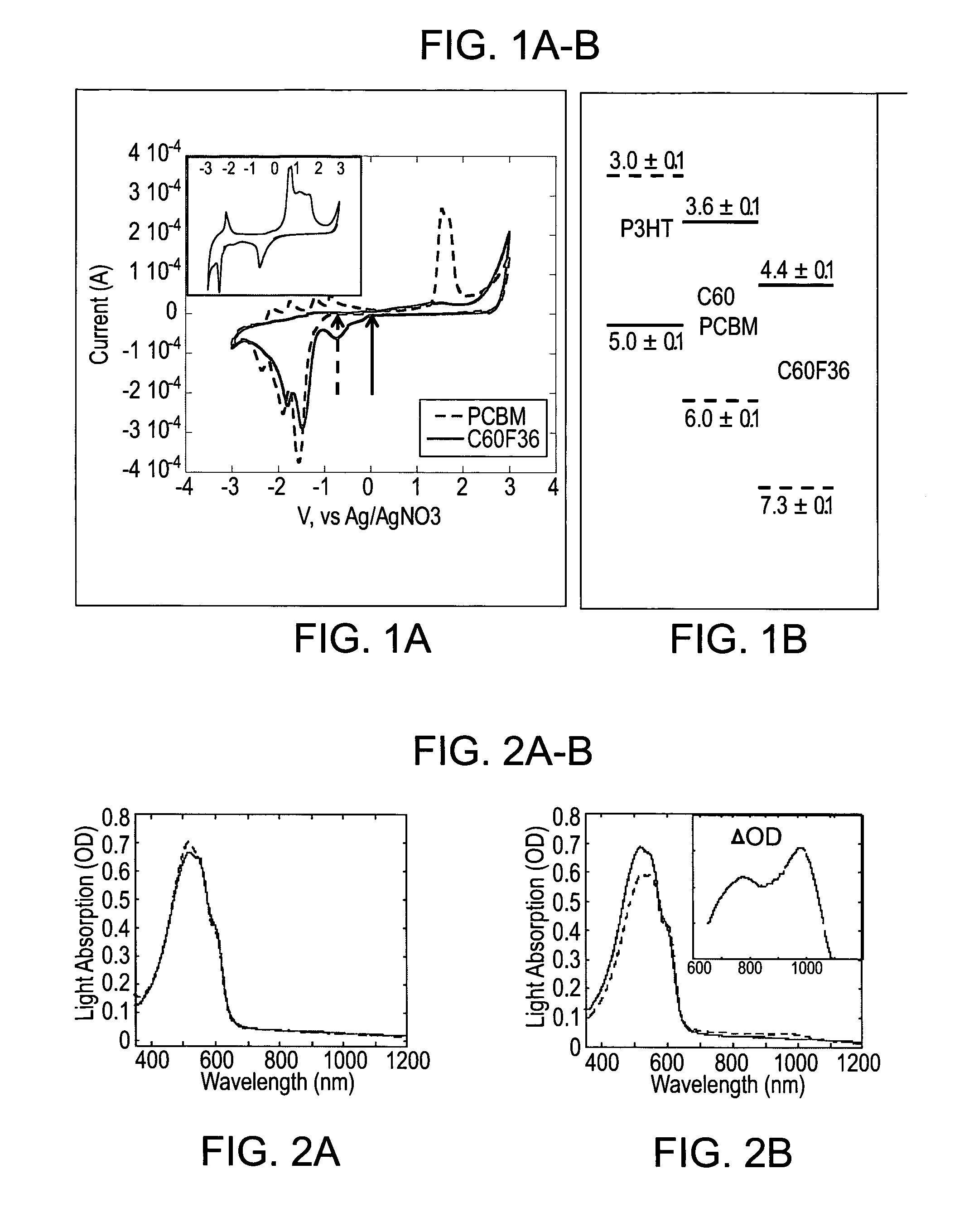
[0187]Cyclic voltammetry (CV) was used for the potentiodynamic electrochemical measurements of the electrochemical properties of the analytes in the form of thin films.

[0188]Generally, the polymer films were fabricated by spin-coating a blend of P3HT / fullerene in 90 / 10, 99 / 1, 99.9 / 0.1, 99.99 / 0.01 and 100 / 0 weight percent ratios respectively. P3HT was first dissolved in 1,2-dichlorobenzene (DCB) to afford a 20 mg / ml solution, followed by blending with 20 mg / ml solution of C60F36 or ...

example 2

Charge-Polaron Induced Absorption in Doped Systems

[0194]A known signature of charge transfer in OSC conjugated polymers is the appearance of a new absorption band associated with charge-polaron induced absorption. Polarons are quasiparticles composed of an electron and a polarization field associated therewith. Polarons are formed when a charge within a molecular chain influences the local nuclear geometry, causing an attenuation or even reversal of nearby bond alternation amplitudes, constituting an excited state which possesses an energy level between the lower and upper energy level bands.

[0195]In order to measure the effect of doping of an OSC polymer with a fluorinated fullerene derivative according to embodiments of the present invention, the absorption spectrum of various systems was recorded and compared as follows.

[0196]Polymer films (and blends of OSC and fullerenes) were prepared as described in Example 1 hereinabove. Absorption spectra were measured using UV-Vis-IR spect...

example 3

Visual Effects in Doped Systems

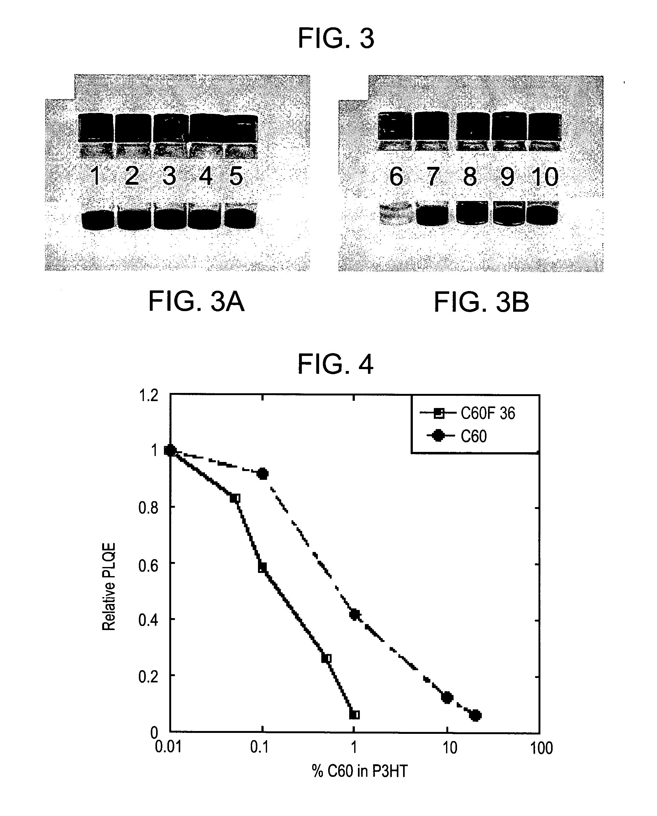
[0200]In order to demonstrate the visual effect of p-doping by fluorinated fullerene derivatives according to embodiments of the present invention, two sets of solutions containing an OSC polymer (P3HT) mixed with a non-fluorinated fullerene (C60) and a fluorinated fullerene (C60F36) in dichlorobenzene (DCB) were compared by visual inspection, and the results are presented in FIGS. 3A-B.

[0201]FIGS. 3A-B are color photographs of two sets of vials, wherein vial No. 1 contains C60 (20 mg in 1 ml of DCB); vial No. 2 contains P3HT (20 mg in 1 ml of DCB); vial No. 3 contains P3HT (20 mg in 1 ml of DCB) mixed with C60 (2 mg or 10% by weight); vial No. 4 contains P3HT (20 mg in 1 ml of DCB) mixed with C60 (0.2 mg or 1% by weight); vial No. 5 contains P3HT (20 mg in 1 ml of DCB) mixed with C60 (0.002 mg or 0.01% by weight); vial No. 6 contains C60F36 (20 mg in 1 ml of DCB); vial No. 7 contains P3HT (20 mg in 1 ml of DCB); vial No. 8 contains P3HT (20 mg in 1 ml...


PUM

PropertyMeasurementUnit
energy levelaaaaaaaaaa

Abstract

Methods for producing p-doped organic semiconductor material with a fullerene derivative having at least one electron-withdrawing substituent covalently attached thereto, and semiconductor compositions prepared thereby are provided. Also provided are electronic devices, such as transistors, solar-cells, illuminating devices, OLEDs and detectors, comprised of these p-doped organic semiconductor materials.

Description

FIELD AND BACKGROUND OF THE INVENTION[0001]The present invention, in some embodiments thereof, relates to applied materials and more particularly, but not exclusively, to novel dopants of organic semiconductors.[0002]Organic semiconductors (OSCs) are taking an ever growing part in the field of advanced electronics. OSCs are organic materials that have semiconductor properties, namely an electrical conductivity between that of typical metals and that of insulating compounds. Organic semiconductors can take the form of single molecules, short chain oligomers and long chain polymers, such as aromatic hydrocarbons, which include pentacene, anthracene and rubrene as semiconductive small molecules, and poly(3-hexylthiophene), poly(p-phenylene vinylene), F8BT, polyacetylene and derivatives thereof as semiconductor oligomers and polymers.[0003]The electron carriers in polymeric OSCs (organic semiconductors in the form of oligomers and polymers) include π-electrons and unpaired electrons, wh...

Claims


Application Information

Patent Timeline
Patent Type & Authority Applications(United States)
IPC IPC(8): H01L51/05H01L51/40H01B1/06H01B1/02B82Y30/00
CPCB82Y10/00Y02E10/549C08G2261/3223C08G2261/92C08L65/00H01L51/001H01L51/0036H01L51/0038H01L51/0039H01L51/004H01L51/0042H01L51/0047H01L51/0052H01L51/0059H01L51/0071H01L51/0078H01L51/0508H01L51/42H01L51/50H01L2251/552C08G2261/141Y02P70/50H10K71/164H10K85/146H10K85/141H10K85/114H10K85/115H10K85/113H10K85/215H10K85/615H10K85/631H10K85/657H10K85/311H10K10/488H10K30/00H10K50/00H10K50/18H10K2101/30H10K85/00
Inventor TESSLER, NIRSOLOMESHCH, OLGA
Owner TECHNION RES & DEV FOUND LTD
Why Eureka
Try Eureka