
Method and system for manipulating organic nanostructures

Inactive Publication Date: 2011-06-30
RAMOT AT TEL AVIV UNIV LTD +2
View PDF0 Cites 8 Cited by
  • Summary
  • Abstract
  • Description
  • Claims
  • Application Information

AI Technical Summary

Benefits of technology

According to some embodiments of the invention at least one of the electronic devices is a field-effect transistor, wherein the gap is between a source electrode and a drain electrode of the field-effect transistor.
Unless otherwise defined, all technical and/or scientific terms used herein have the same meaning as commonly understood by one of ordinary skill in the art to which the invention pertains. Alt

Problems solved by technology

Traditionally, microscopic devices have been formed from larger objects, but as these products get smaller, below the micron level, this process becomes increasingly difficult.

Method used


Image

  • Method and system for manipulating organic nanostructures
  • Method and system for manipulating organic nanostructures
  • Method and system for manipulating organic nanostructures

Examples


example 1

This Example describes experiments in which peptide nanotubes were immobilized onto electrode structures by dielectrophoresis (DEP), according to some embodiments of the present invention.

Materials and Methods

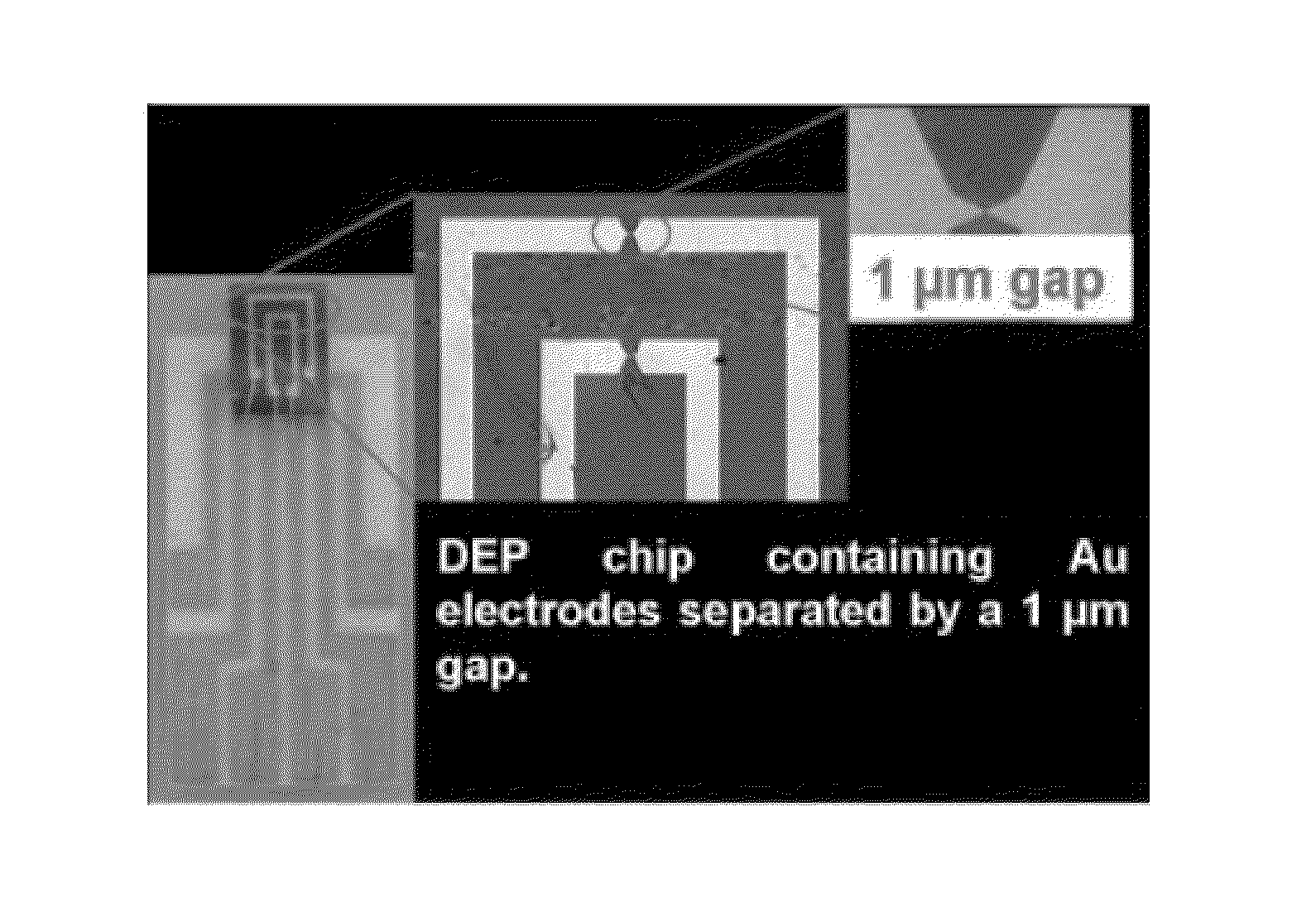
A DEP microchip was fabricated according to some embodiments of the present invention by optical lithography on a silicon wafer following a protocol previously described in Dimaki, M. and Boggild, P., Nanotechnology 2005, 16, 759-763. Briefly, SiO2 was grown on top of a silicon wafer as an insulating layer. A 1.5 m resist layer was spun on top of the oxide and a positive photolithography process was used in order to pattern the electrodes on the oxide. After development of the resistance 10 nm of titanium and 150 nm of gold were deposited on the wafer and a lift-off process using acetone was carried out to define the electrodes. The titanium layer enhanced the adhesion between the gold and the silicon oxide layer. FIG. 4A illustrates the fabrication steps. The final DEP microch...

example 2

This Example describes experiments performed according to some embodiments of the present invention for qualitative mapping of structurally different polypeptide nanotubes.

Electrostatic force microscopy (SPM) was used to distinguish between diphenylalanine nanotubes, silver filled nanotubes and silver wires placed on pre-fabricated SiO2 surfaces with a backgate. Substrates for the experiments were fabricated by the use of four inch 350 μm thick heavily p-doped silicon wafers. A 100 nm thick silicon oxide layer was grown on the substrates, the oxide on the back was removed by HF and a 20 nm layer was evaporated on the backside followed by a 500 nm layer of gold. For the casting of silver nanowires inside the peptide nanotubes an aliquot of 10 μL, of a boiling solution of AgNO3 was added to 90 μL, of a peptide nanotubes solution (aged for 1 night). After this 6 μL, of a solution of 1% citric acid was added until a final concentration of 0.038% citric acid was reached to serve as a red...

example 3

This example describes experiments performed according to some embodiments of the present invention for electrochemical characterization of four types of 8-amino acid peptide nanofibers, referred to below as NS, NC, CN and CS. The amino acid sequence of each type of nanofibers is listed in Table 3, below.

TABLE 3NSH2N-Asn-Ser-Gly-Ala-Ile-Thr-Ile-Gly-CONH2(SEQ ID NO: 1)NCH2N-Asn-Cys-Gly-Ala-Ile-Thr-Ile-Gly-CONH2(SEQ ID NO: 2)CNH2N-Cys-Asn-Gly-Ala-Ile-Thr-Ile-Gly-CONH2(SEQ ID NO: 3)CSH2N-Cys-Ser-Gly-Ala-Ile-Thr-Ile-Gly-CONH2(SEQ ID NO: 4)

The nanofibers are formed by dissolving different amounts of the peptide powder in distilled water at room temperature. Samples are incubated at room temperature during 4 days to get a higher density of nanofibers. As representative examples, SEM images of the NC and CN nanofibers are shown in FIGS. 16A-B, respectively.

Nanofibers and gold modified nanofibers were evaluated by cyclic voltammetry (CV) on different working electrodes, graphite, gold and p...


PUM

PropertyMeasurementUnit
Frequencyaaaaaaaaaa
Frequencyaaaaaaaaaa
Concentrationaaaaaaaaaa

Abstract

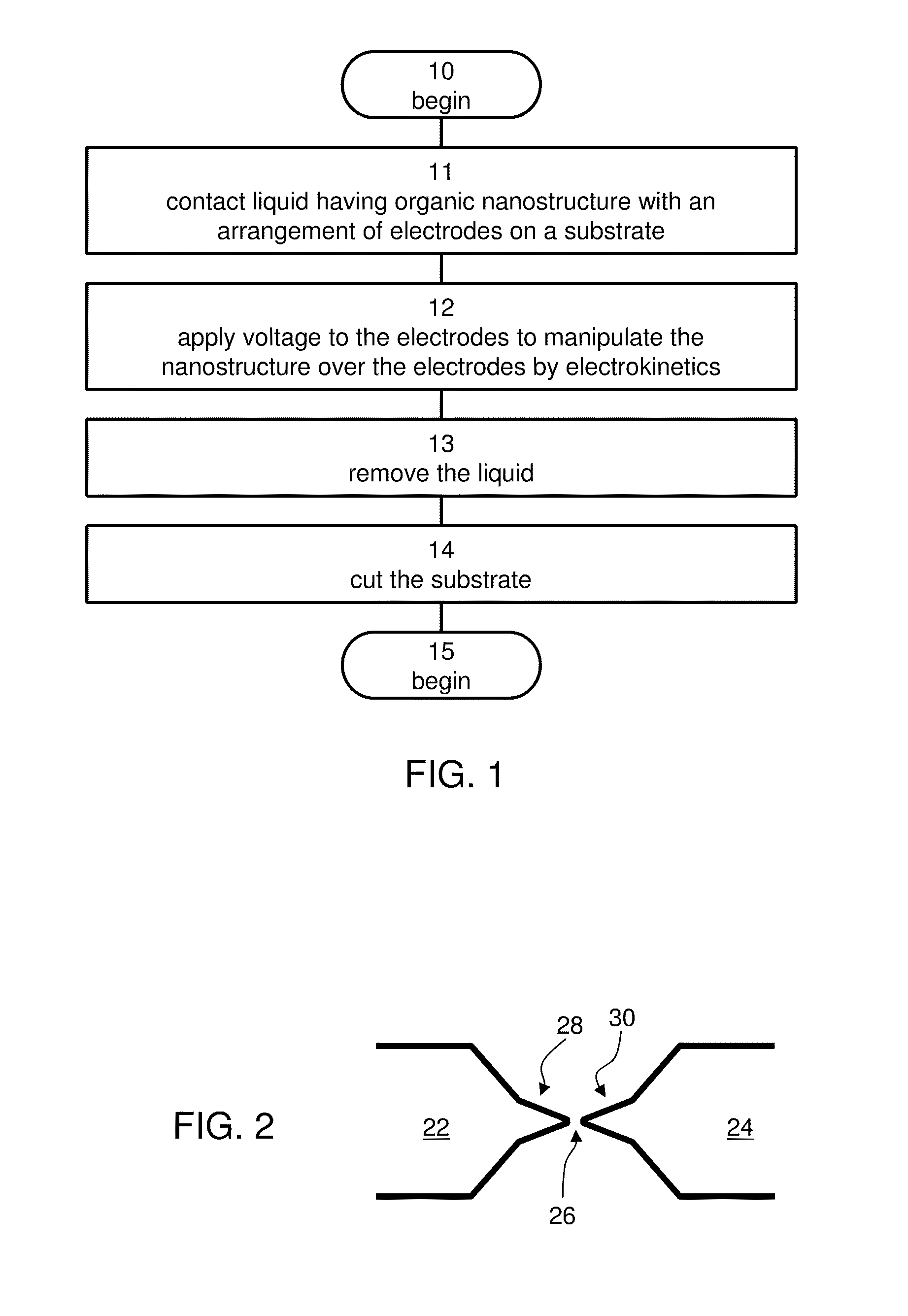
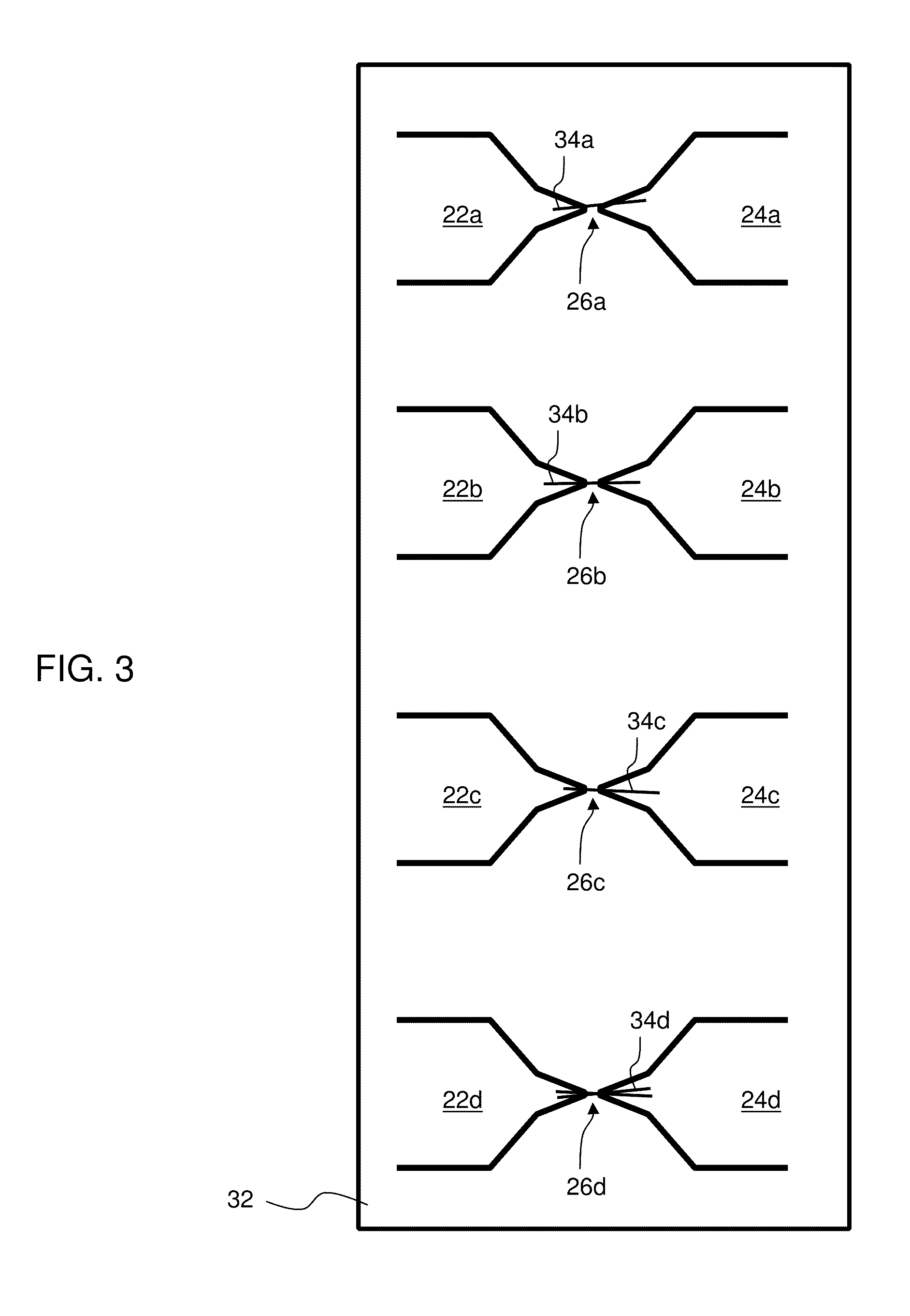
A method of manipulating an organic nanostructure is disclosed. The method comprises: contacting a liquid sample having the organic nanostructure therein with an arrangement of electrodes, and applying voltage to the arrangement of electrodes to manipulate and immobilize the organic nanostructure over the electrodes by electrokinetics.

Description

FIELD AND BACKGROUND OF THE INVENTIONThe present invention, in some embodiments thereof, relates to nanotechnology and, more particularly, but not exclusively, to a method and system for manipulating organic nanostructures.It is well established that future development of devices such as microelectronics devices and chemical sensors will be achieved by increasing the packing density of device components. Traditionally, microscopic devices have been formed from larger objects, but as these products get smaller, below the micron level, this process becomes increasingly difficult. It is therefore appreciated that the opposite approach is to be employed, essentially, the building of microscopic devices via objects of nanometric dimensions.In particular, nanostructures of elongated shape have attracted extensive interest due to their great potential for addressing some basic issues about dimensionality and space confined transport phenomena as well as related applications.Numerous config...

Claims


Application Information

Patent Timeline
IPC IPC(8): H01L29/772C25B9/00
CPCB82Y5/00B82Y10/00H01L51/0093C07K5/06078B82Y40/00H10K85/761
Inventor GAZIT, EHUDADLER-ABRAMOVICH, LIHICASTILLO LEON, JAIME ALBERTODIMAKI, MARIA IOANNOUSVENDSEN, WINNIE EDITHKASOTAKIS, EMMANOUILMITRAKI, ANNA
Owner RAMOT AT TEL AVIV UNIV LTD
Learn More