Method for manufacturing twin bit structure cell with hafnium oxide and nano-crystalline silicon layer

a technology of hafnium oxide and nano-crystalline silicon, applied in the direction of semiconductor devices, electrical equipment, basic electric elements, etc., can solve the problems of complex manufacturing process, high cost of integrated circuit or chip fabrication facilities, and difficulty in small devices, so as to achieve a broader range of application.

Inactive Publication Date: 2011-06-30
SEMICON MFG INT (SHANGHAI) CORP +1
View PDF37 Cites 11 Cited by
  • Summary
  • Abstract
  • Description
  • Claims
  • Application Information

AI Technical Summary

Benefits of technology

[0007]Embodiments of the present invention provide innovative techniques of manufacturing memory devices. More particularly, embodiments according to the present invention provide a method and a design for manufacturing a twin bit cell structure for a non-volatile memory device. But it should be recognized that the present invention has a much broader range of applicability.

Problems solved by technology

An integrated circuit or chip fabrication facility can cost hundreds of millions, or even billions, of U.S. dollars.
Making devices smaller is very challenging, as each process used in the fabrication of integrated circuits has a limit.
An example of such limitation lies in the manufacturing of memory devices.
As the feature size continues to shrink, a twin bit cell structure will become more difficult to design and manufacture as it is difficult to control the gates independently.
One of the challenges in the semiconductor processing has been the manufacturing of twin-bit cell structures for non-volatile memory devices, such as the widely used flash based memory devices.
Among other things, the conventional system and method for manufacturing cells with twin-bit structures face limitations when further scaling down of the cell size is required.

Method used


Image

  • Method for manufacturing twin bit structure cell with hafnium oxide and nano-crystalline silicon layer
  • Method for manufacturing twin bit structure cell with hafnium oxide and nano-crystalline silicon layer
  • Method for manufacturing twin bit structure cell with hafnium oxide and nano-crystalline silicon layer

Examples


Embodiment Construction

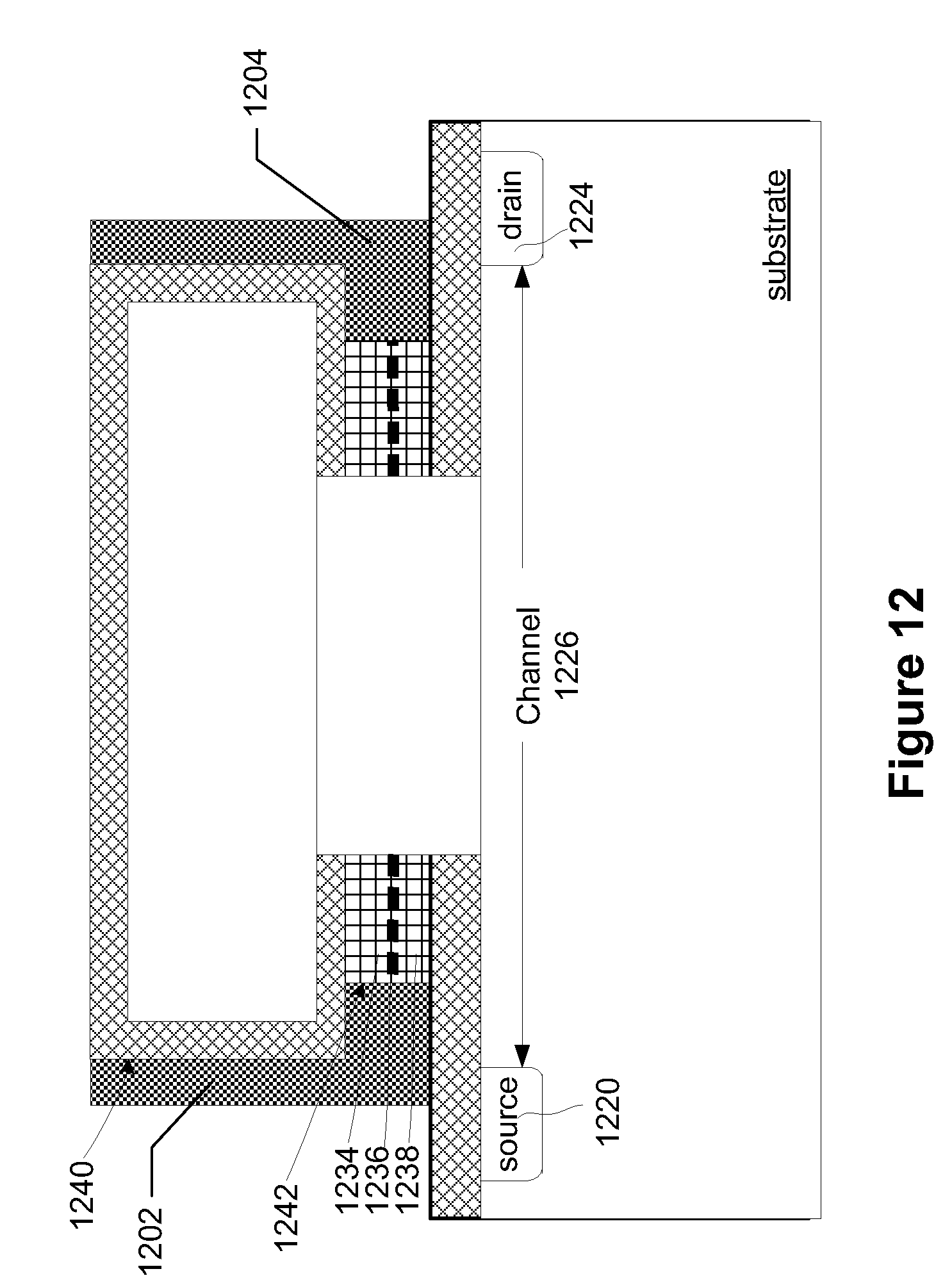
[0018]Embodiments of the present invention provide techniques for manufacturing non-volatile memory devices. Merely by way of example, embodiments according to the present invention provide a method and a design for manufacturing a twin bit cell structure of a non-volatile memory device. But embodiments according to the present invention can also be applied to manufacturing of other devices.

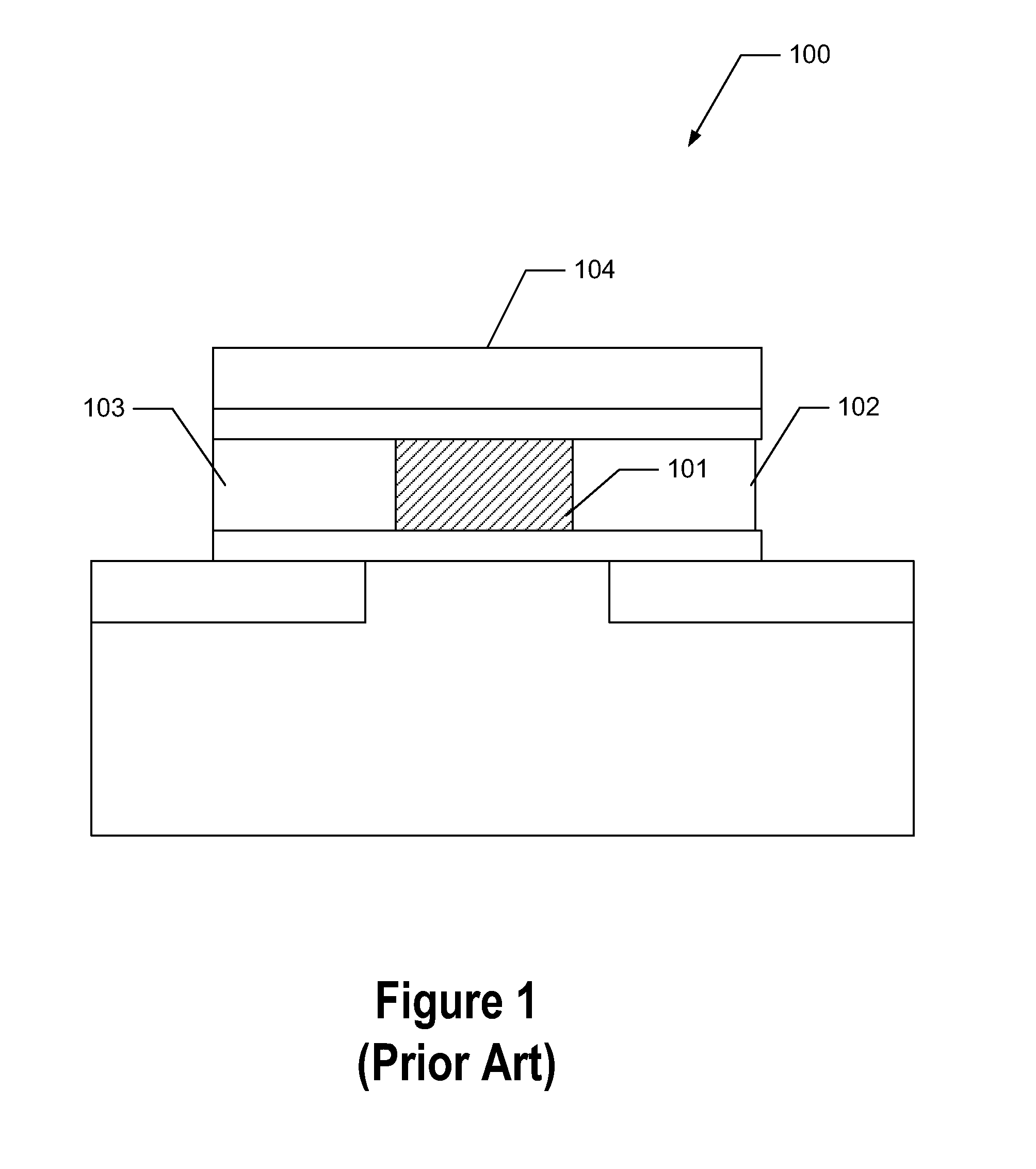
[0019]FIG. 1 is a simplified twin bit cell structure using a conventional method of fabrication. As shown in FIG. 1, the twin-bit structure 100 has two conductive regions 102 and 103 that can be configured to hold charges. The two conductive regions are separated by an isolation region 101. A control gate 104 overlays the conductive regions.

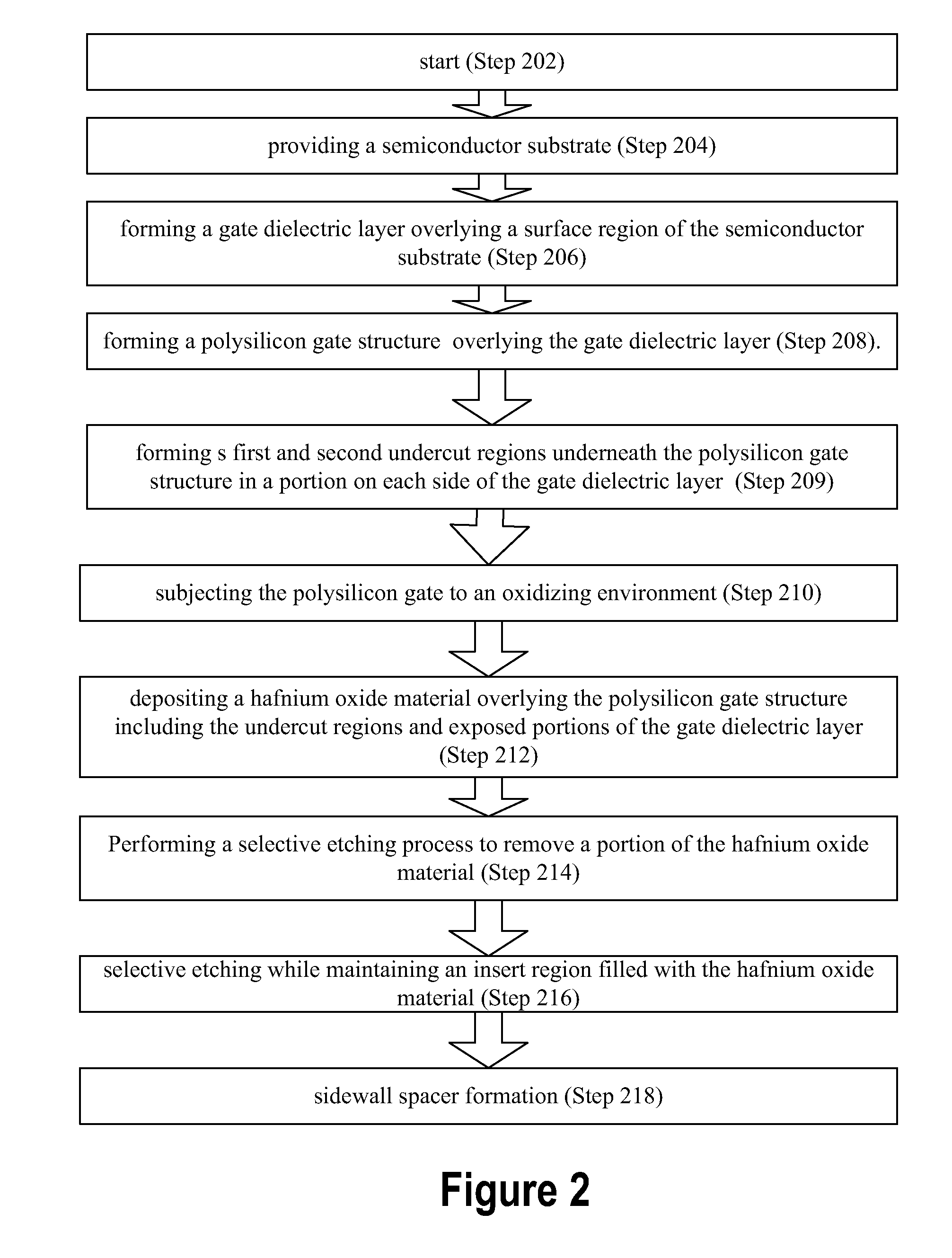
[0020]As an example, the twin bit cell structure shown in FIG. 1 is manufactured using the following steps:

[0021]1. provide a p-type substrate;

[0022]2. form a gate oxide layer overlaying the substrate;

[0023]3. form an n-type doped polysilicon layer;

[0024]4. fo...


PUM


Abstract

A method and system for forming a non-volatile memory structure. The method provides a semiconductor substrate and forms a gate dielectric layer overlying a surface region of the semiconductor substrate. A polysilicon gate structure is formed overlying the gate dielectric layer. The method subjects the polysilicon gate structure to an oxidizing environment to cause formation of a first silicon oxide layer overlying the polysilicon gate structure and formation of a second silicon oxide layer overlying a surface region of the substrate. A hafnium oxide material is formed overlying the first and second silicon oxide layers and filling the undercut region. The hafnium oxide material has a nanocrystalline silicon material sandwiched between a first hafnium oxide layer and a second hafnium oxide layer. The hafnium oxide material is selectively etched while a portion of it is maintained in an insert region in a portion of the undercut region.

Description

CROSS-REFERENCES TO RELATED APPLICATIONS[0001]This application claims priority to Chinese Application No. 200910247494.2; filed on Sep. 12, 2009; which is commonly owned and incorporated by reference herein for all purposes.BACKGROUND OF THE INVENTION[0002]Embodiments of the present invention relate to integrated circuits and the processing for the manufacture of semiconductor devices. More particularly, embodiments of the invention provide a method and a device for forming a twin bit cell structure for semiconductor integrated circuit devices, but it would be recognized that the invention has a much broader range of applicability. In a specific embodiment, the present invention provides a method for manufacturing a twin-bit structure cell with a hafnium oxide layer and a nano-crystalline silicon layer that are used together for storing charges.[0003]Integrated circuits have evolved from a handful of interconnected devices fabricated on a single chip of silicon to millions of device...

Claims


Application Information

Patent Timeline
Patent Type & Authority Applications(United States)
IPC IPC(8): H01L29/792H01L21/336
CPCH01L21/28282H01L29/7923H01L29/66833H01L29/40117
Inventor FUMITAKE, MIENO
Owner SEMICON MFG INT (SHANGHAI) CORP
Why Eureka
Try Eureka