Patterning method

a patterned layer and pattern technology, applied in the field of patterning methods, can solve the problems of dimensional changes within a single patterned layer, registration errors may accumulate between tft layers, and changes in the dimensions of the carrier substrate, so as to reduce parasitic capacitance, accurate alignment, and improve device speed

Inactive Publication Date: 2011-06-30
EASTMAN KODAK CO
View PDF4 Cites 6 Cited by
  • Summary
  • Abstract
  • Description
  • Claims
  • Application Information

AI Technical Summary

Benefits of technology

[0016]The method of the invention is self-aligning. It is insensitive to substrate distortion and very accurately aligns, for example, the gate electrode of a TFT to the semiconductor channel region between the source and drain electrodes with no overlap. This reduces parasitic capacitance and improves device speed.
[0017]The invention allows the distance between the source and drain electrodes (i.e. the semiconductor channel length) to be reduced substantially below printing resolutions. It enables gaps to be brought much closer with respect to the width of an inkjet droplet. Bringing the lines closer together reduces TFT conduction path length thus increasing switching speeds and reducing the device footprint.
[0018]The method of the invention also increases the speed of forming the patterns. It is possible to deposit a functional fluid into a well or deposition region and have the patterns form by virtue of capillary flow whilst the deposition head is being moved to the next well. It is not necessary to actually deposit fluid at all points the fluid is required.
[0019]The invention provides better adhesion of overlayers to the substrate since it does not have to have a lyophobic characteristic on the areas where the flowable material should not flow. There is no possibility for the deposition region to empty and create open circuits. There is no possibility for the channel to overflow and create short circuits. The closest approach of two channels can be much closer because there is no need to have a large lyophobic land between the channels.
[0020]The invention also allows the pre-patterning step to be simplified. There is no requirement for, for example, the formation of banks or areas of surface energy contrast. In the preferred embodiment channels are defined as recessed regions in the surface and may be formed for example by photolithography, embossing, laser ablation, cutting and moulding. In a further preferred embodiment, embossing alone is enough to prepare the substrate for patterning. Embossing is a low cost technique and may be done roll-to-roll so that incremental costs in preparing the substrate for deposition are minimised versus some of the other routes.
[0021]The method of the invention may be readily used to pattern functional materials to achieve feature sizes of 100 nm. With great care and careful selection of materials it is possible to make patterns by the method with feature sizes of a few tens of nanometres. The method enables very high resolution features to be made and is therefore applicable to the manufacture of frequency selective surfaces, metamaterials, as well as all kinds of electronic devices and optoelectronic devices. The method of the invention may also be used to pattern biological materials and to make sensor arrays.

Problems solved by technology

Between each step and even during a step, environmental conditions such as ambient temperature and, humidity may change, causing changes in dimensions of the carrier substrate for the TFTs and of masks or positioning equipment for deposition or patterning tools.
Thus registration errors may accumulate between TFT layers.
These temperature changes also cause dimensional changes within a single patterned layer and again registration may be affected.
Another important issue to be considered is the efficient use of materials.
This subtractive approach, while highly reliable and accurate, is wasteful of materials.
For small feature sizes, however, additive processes, such as conventional printing and inkjet have more limited applicability.
This significantly limits the resolution of patterning that can be achieved.
Furthermore, there is a limit to the accuracy with which inkjet droplets can be placed at a precise location on a surface.
A further difficulty is the use of raised topologies in some embodiments which suffer greatly reduced capillary flow speed's due to the convex profile of the surface of the liquid as it flows along the channel.
Managing the flow of liquid on the surface of the substrate on which the electronic devices are fabricated is a key issue, especially given the need to reduce processing time to a minimum so that fabrication costs are low.
Furthermore, it is generally much harder to get good adhesion between a lyophobic surface and a layer that is deposited on top of it.

Method used


Image

  • Patterning method
  • Patterning method
  • Patterning method

Examples


example 1

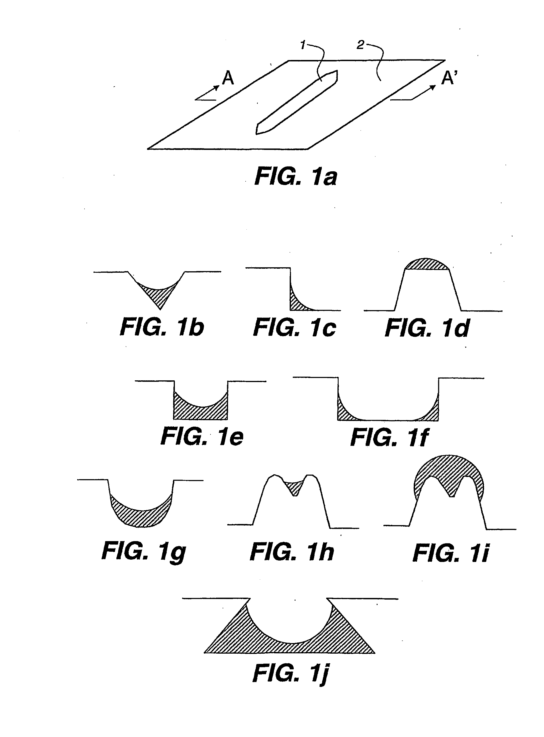
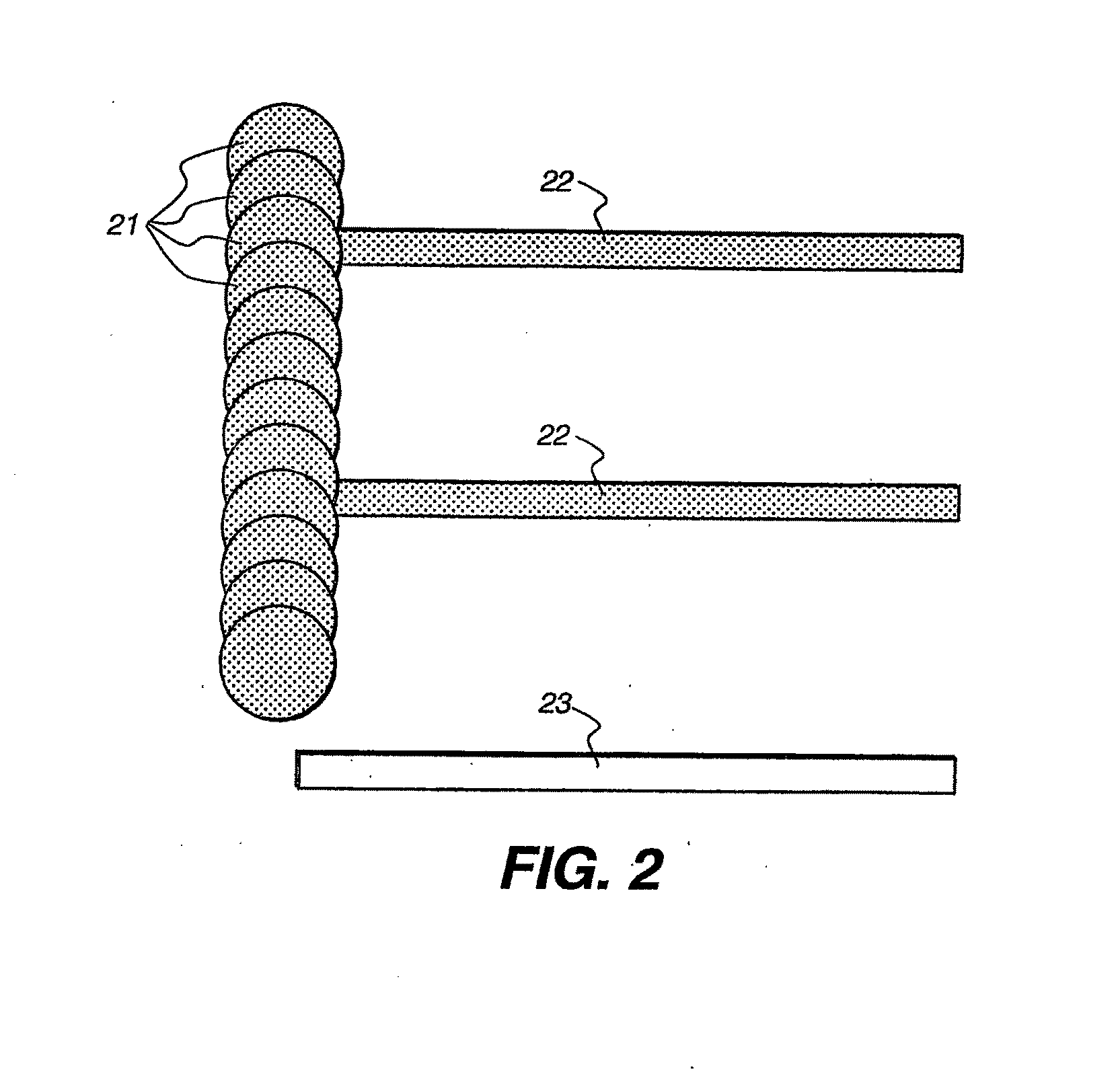
[0050]In FIG. 3 the black areas are channels 33 created in photoresist, with a width of 50-200 micrometers and a depth of 50 micrometers. The large black squares are the ‘deposition regions’34 into which the functional liquid is deposited by ink jet. Capillary forces then cause the liquid to flow into the channels.

[0051]The behaviour of the liquid is determined by the contact angle between the liquid and the substrate in which the channels are fabricated. Two angles are of importance here; the advancing angle, which determines whether the liquid will wet the substrate and be drawn into the channel, and the receding angle, which determines whether the substrate will remain wetted by the liquid, or if the liquid will de-wet. This is important if a design such as that shown in FIG. 3 is used to create conductive pads for an electrical device. Ideally one would like the ‘deposition regions’ (black squares) to remain wetted by the liquid, to allow for subsequent electrical connection to ...

example 2

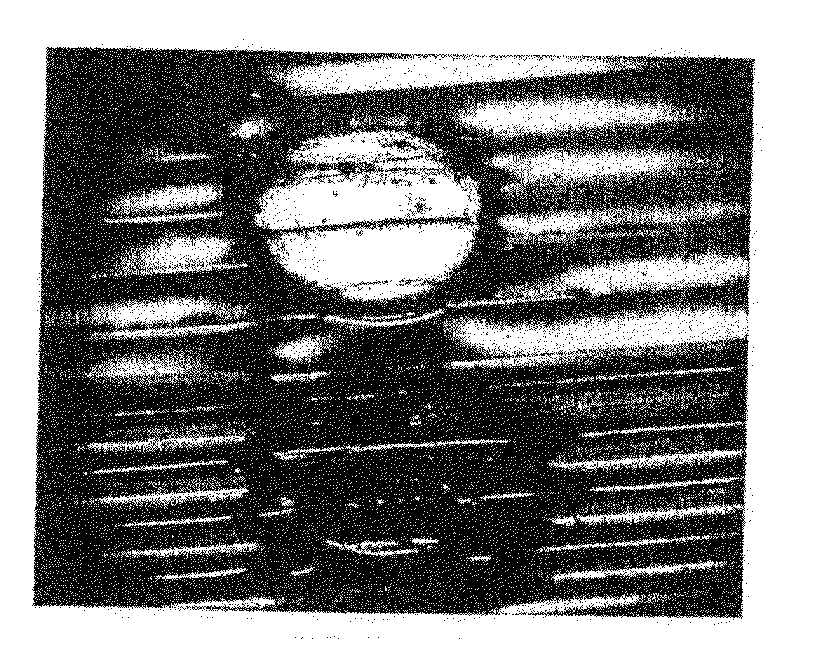
[0053]In this example V shaped grooves in polycarbonate (3M optical lighting film, SOLF™) were used as the substrate material as shown in FIG. 4. FIG. 4a shows schematically the apex of each groove 41 and two deposition regions 42 and 43 defined in the substrate. The untreated polycarbonate material has an advancing contact angle of ˜70 deg. and a receding angle of ˜65 deg. with water. The high advancing angle causes the water to not freely wet the polycarbonate, and so it was not drawn along the grooves.

[0054]The test liquid used was a non-drying ink used as a model fluid with constituents;

Water+

[0055]Diethylene glycol—14-22%

Black colourant 13-14%

Butoxy tri glycol 10%

Urea 3-6%

Triethanolamine 1-3%

[0056]The solution as used had a viscosity of a few cP and a surface tension of approximately 30 mNm−1.

[0057]The advancing contact angle and receding contact angle of the test liquid on the polycarbonate substrate were both approximately 30 degrees. It was found that the liquid would wick a...


PUM

PropertyMeasurementUnit
contact angleaaaaaaaaaa
receding contact angleaaaaaaaaaa

Abstract

The invention provides a method of patterning flowable material on a surface. The method comprises providing the surface with at least one channel and at least one deposition region connected to the at least one channel, the width of the channel being less than the width of the deposition region, and depositing flowable material in the deposition region such that when the material makes contact with the channel the material is directed into said channel by capillary forces, the receding contact angle of the flowable material in the deposition region being less than 30°.

Description

FIELD OF THE INVENTION[0001]The invention relates to a patterning method and in particular to a method of patterning a surface in the manufacture of electronic, optical and optoelectronic devices. The invention also relates to devices manufactured by the method.BACKGROUND OF THE INVENTION[0002]The development of silicon-based thin-film transistor (TFT) technology has been an essential enabler for the development of large flat panel displays. Despite the huge cost of factories to manufacture TFTs on glass and the complexity of the TFT manufacturing process, the technology is now well-established for active matrix liquid crystal displays and is based largely on photolithographic techniques for depositing patterns of the various materials into multilayer structures.[0003]In recent years great progress has been made on TFT technologies based on other semiconductors including polymers, metal oxides and semiconducting nanowires and nanotubes. Many of these approaches benefit from simpler ...

Claims


Application Information

Patent Timeline
Patent Type & Authority Applications(United States)
IPC IPC(8): B32B3/10B05D5/00B05D1/00B05D5/12
CPCB82Y10/00B82Y40/00Y10T428/24802H01L51/0004H01L27/1292G03F7/0002H10K71/13
Inventor RIDER, CHRISTOPHER B.CLARKE, ANDREW
Owner EASTMAN KODAK CO
Why Eureka
Try Eureka