LED units fabrication method

a technology of fabrication method and led unit, which is applied in the direction of basic electric elements, electrical equipment, semiconductor devices, etc., can solve the problems of thin gan epitaxial layer buckles or cracks, and it is difficult to separate individual devices from the sapphire substra

Inactive Publication Date: 2011-06-30
HON HAI PRECISION IND CO LTD
View PDF7 Cites 111 Cited by
  • Summary
  • Abstract
  • Description
  • Claims
  • Application Information

AI Technical Summary

Problems solved by technology

However, because the sapphire substrate is hard, chemically resistant, and has no natural cleave angles, it is very difficult to separate the individual devices from the sapphire substrate.
However, the thin GaN epitaxial layer may buckle or crack during the LLO process, because it is usually not strong enough to withstand a high-energy laser shock wave.

Method used


Image

  • LED units fabrication method
  • LED units fabrication method
  • LED units fabrication method

Examples


Embodiment Construction

[0011]Referring to FIG. 1, an embodiment of a method for fabricating LED units is described as follows:

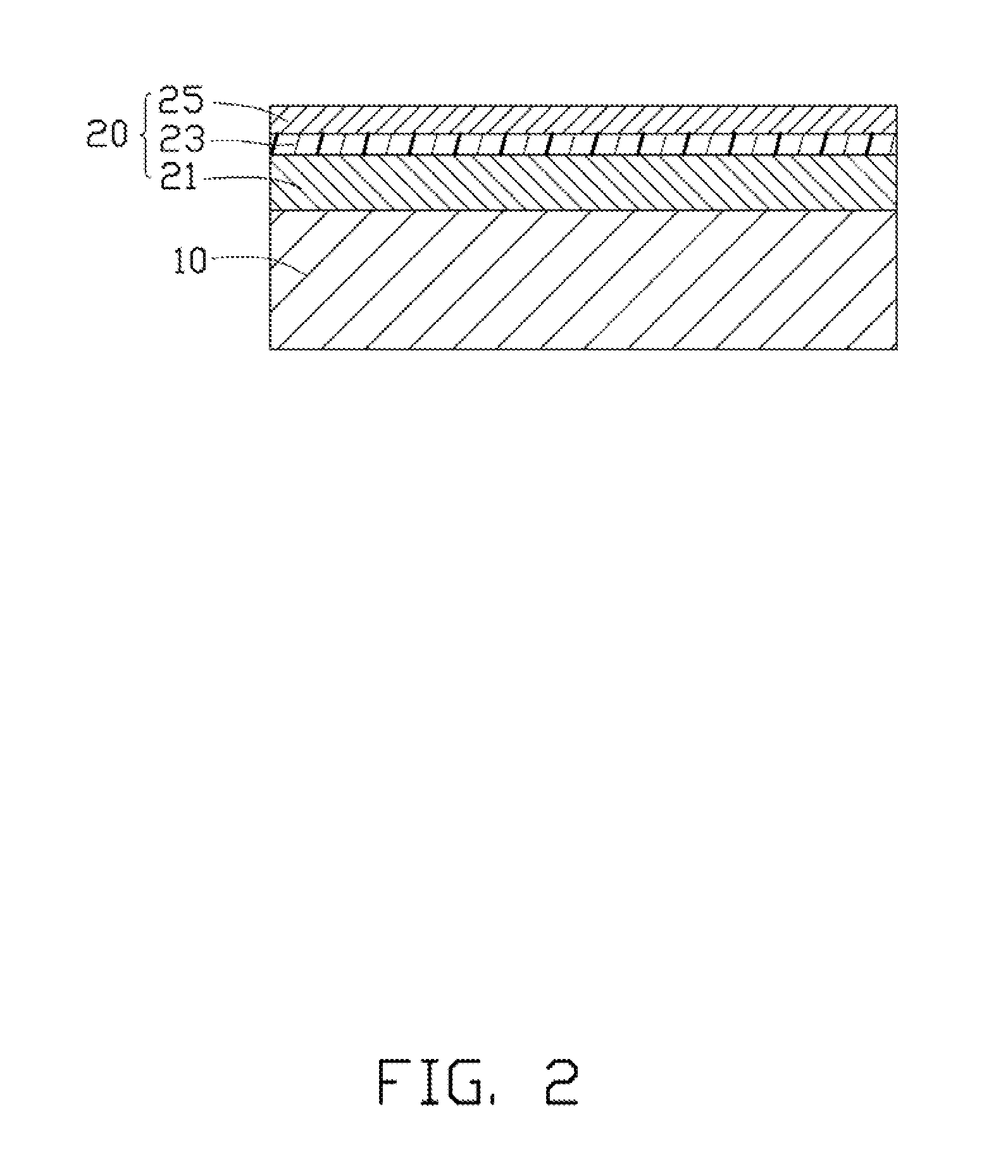
[0012]In step S1, a sapphire substrate 10, which has a round flat surface, is provided.

[0013]In step S2, referring to FIG. 2, a GaN epitaxial layer 20 is formed on the flat surface of the sapphire substrate 10. In one embodiment, the GaN epitaxial layer 20 is formed using metal organic chemical vapor deposition (MOCVD). The GaN epitaxial layer 20 includes a lamination of an n-GaN layer 21, an active layer 23, and a p-GaN layer 25. In alternative embodiments, the GaN epitaxial layer 20 may also be formed with other appropriate epitaxial growth methods, such as molecular beam epitaxy (MBE) or hydride vapor phase epitaxy (HYPE).

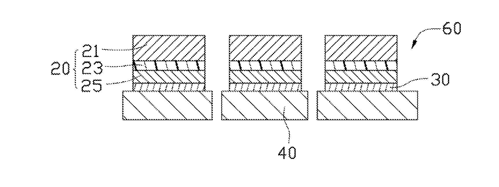
[0014]In step S3, referring to FIG. 3, a plurality of exhaust trenches 27 is formed in the GaN epitaxial layer 20 using reactive ion etching, preferably inductively coupled plasma (ICP) reactive ion etching. The exhaust trenches 27 pass through the n-GaN layer ...


PUM


Abstract

A method for fabricating a plurality of individual light emitting diode units includes forming a GaN epitaxial layer on a sapphire substrate, forming a plurality of exhaust trenches on the GaN epitaxial layer, wherein the exhaust trenches define a plurality of individual light emitting diode units, forming a reflective layer on the GaN epitaxial layer, attaching the reflective layer to a conductive substrate, removing the sapphire substrate from the GaN epitaxial layer via a laser lift-off process, wherein a gas produced during the laser lift-off process is exhausted via the exhaust trenches, and dicing the conductive substrate along the exhaust trenches to form the plurality of individual light emitting diode units.

Description

TECHNICAL FIELD[0001]The present disclosure relates generally to a LED units fabrication method.DESCRIPTION OF RELATED ART[0002]Light emitting diodes (LEDs) are well-known semiconductor devices that convert current into light. The color of the light (wavelength) emitted by an LED depends on the semiconductor materials used. Gallium-Nitride (GaN) has gained much attention, because it is found that GaN can be combined with indium to produce InGaN / GaN semiconductor layers that can emit green, blue, and ultraviolet light. This wavelength controllability enables an LED semiconductor designer to tailor material characteristics to achieve beneficial device characteristics. Accordingly, GaN-based opto-electronic device technology has rapidly evolved since their commercial introduction in 1994.[0003]Sapphire substrates are typically used as a base in the fabrication of GaN-based LEDs. Fabricating LEDs on the sapphire substrate is typically performed by growing a GaN epitaxial layer on the sa...

Claims


Application Information

Patent Timeline
Patent Type & Authority Applications(United States)
IPC IPC(8): H01L21/30
CPCH01L33/0079H01L33/0093
Inventor LAI, CHIH-CHEN
Owner HON HAI PRECISION IND CO LTD
Why Eureka
Try Eureka