Food quality examination device, food component examination device, foreign matter component examination device, taste examination device, and changed state examination device

a technology of examination device and foreign matter, which is applied in the direction of optical radiation measurement, radiation control device, instruments, etc., can solve the problems of high noise, increase the cost of the device, and disadvantageous dark current at wavelengths of 2.5 m or less of pds, and achieve high sensitivity

Active Publication Date: 2011-07-14
SUMITOMO ELECTRIC IND LTD
View PDF3 Cites 12 Cited by
  • Summary
  • Abstract
  • Description
  • Claims
  • Application Information

AI Technical Summary

Benefits of technology

[0063]According to the present invention, it is possible to provide a food quality examination device configured to inspect the quality of food with high sensitivity using an InP-based photodiode in which a dark current is decreased without a cooling mechanism and the sensitivity is extended to a wavelength of 1.8 μm or more. Furthermore, it is possible to provide a food component examination device, a foreign matter component examination device, a taste examination device, and a changed state examination device including the photodiode.

Problems solved by technology

In near-infrared spectroscopy, output signals contain necessary information and high levels of noise attributed to light receiving elements.
Thus, large-scale devices are needed, thereby increasing the cost of the devices.
Although the PDs can be used at room temperature, the PDs disadvantageously have high dark currents at wavelengths of 2.5 μm or less and poor detection capabilities.
The InP-based PDs of item (2) have disadvantages that (I) although InGaAs, which is lattice-matched to InP, has a low dark current, the sensitivity is limited to wavelengths of 1.7 μm or less in the near-infrared region, and (II) extended-InGaAs with sensitivity at extended wavelengths up to 2.6 μm has a high dark current and needs to be cooled.
Thus, InP-based PDs cannot use light having a wavelength of 2.0 μm or more, the light being important in the inspection of food, or needs to be cooled when use the light.
As described above, InGaAs PIN photodiodes have a problem of the need to extend the sensitivities to longer wavelengths in the near-infrared region.
Although the measures for improvement are proposed as described above, the extension of the sensitivity to wavelengths of 1.7 μm or more and the suppression of noise and dark current have not been satisfactorily achieved by any of the measures of items (K1) to (K4).

Method used


Image

  • Food quality examination device, food component examination device, foreign matter component examination device, taste examination device, and changed state examination device
  • Food quality examination device, food component examination device, foreign matter component examination device, taste examination device, and changed state examination device
  • Food quality examination device, food component examination device, foreign matter component examination device, taste examination device, and changed state examination device

Examples


first embodiment

iconductor Light Receiving Element Array—

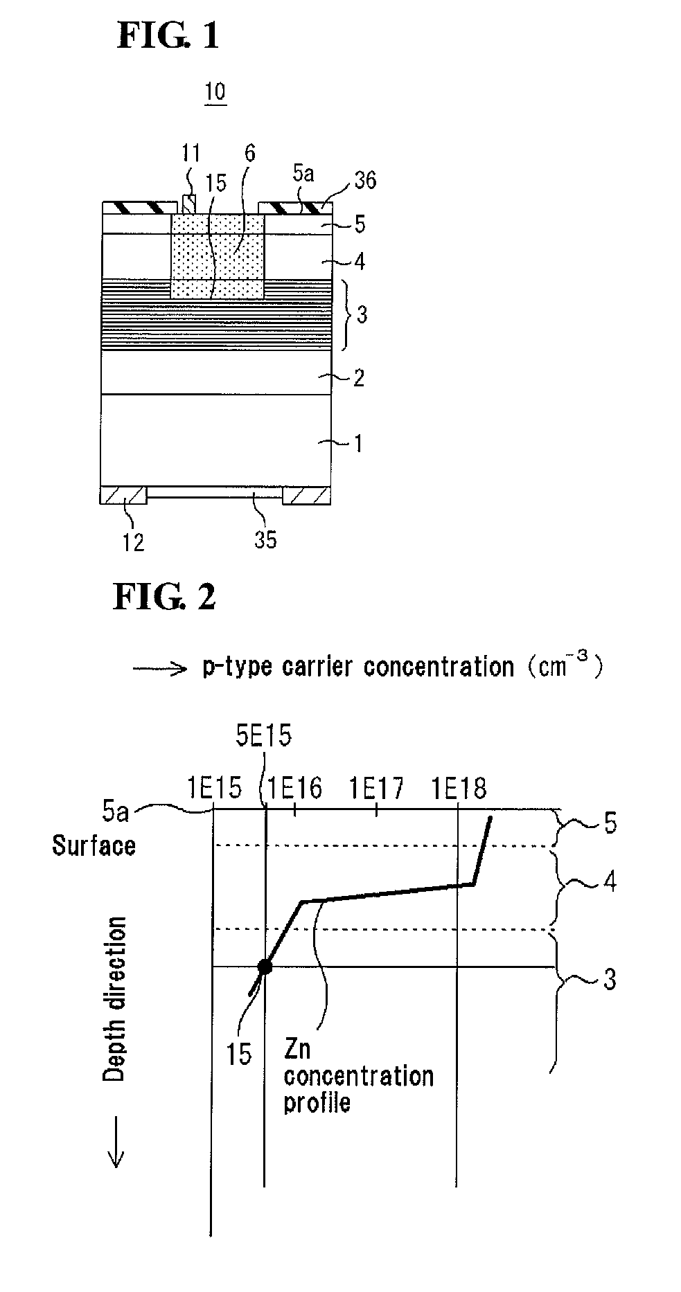
[0091]FIG. 1 is a cross-sectional view of a light receiving element 10 according to an embodiment of the present invention. Referring to FIG. 1, the light receiving element 10 includes a following III-V group semiconductor laminated structure (epitaxial wafer) on an InP substrate 1:[0092](InP substrate 1 / InP buffer layer 2 / absorption layer 3 with a multiquantum well structure composed of InGaAs or GaInNAs and GaAs Sb / InGaAs diffusion concentration distribution control layer 4 / InP window layer 5).

[0093]A p-type region 6 extending from the InP window layer 5 to the absorption layer 3 having the multiquantum well structure is formed by selectively diffusing Zn, which serves as a p-type impurity, through an opening of a selective diffusion mask pattern 36 made of a SiN film. The p-type impurity is introduced by selective diffusion into a portion inner than the peripheral portion of the light receiving element 10 using the selective diffusion mask...

second embodiment

ing Device (Composition Distribution Imaging Device) in Food Composition or Foreign Matter Component Examination Device—

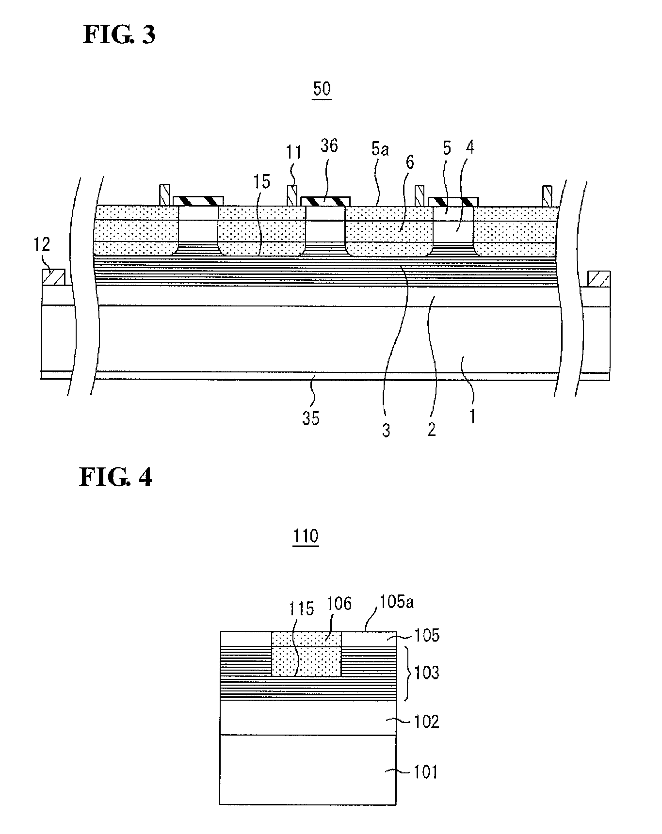
[0119]FIG. 8 illustrates the outline of an imaging device 70 (light receiving element array) included in a food composition or foreign matter component examination device according to a second embodiment of the present invention. Optical components, such as a lens, are omitted. FIG. 9 is an explanatory view of the light receiving element array 50 of the foregoing imaging device. FIG. 10 illustrates one of the light receiving elements 10 in the light receiving element array 50 illustrated in FIG. 9. Referring to FIG. 8, in the case of the imaging device 70, the light receiving elements 10 provided on a common InP substrate 51 are epi-side-down mounted in such a manner that the epitaxial layer sides thereof are adjacent to a multiplexer 71 serving as a mounting substrate. The p-side electrode 11 electrically connected to the p-type region 6 of the epitaxial layer of ...

seventh embodiment

ponent Examination Device—Detection of PCB and so Forth in Fat—

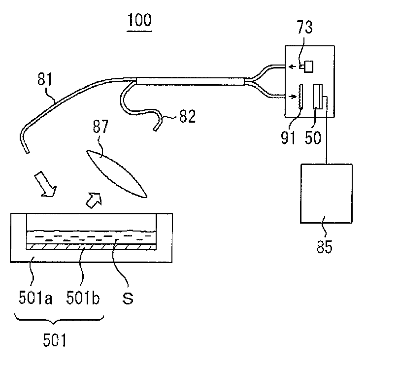
[0140]FIG. 21 illustrates an device for detecting PCB and so forth in fat according to a seventh embodiment of the present invention. In the case of a foreign matter component examination device 100, fat is formed into a liquid by heating or with, for example, an organic solvent or enzyme. Then a halogenated organic compound, in particular, polychlorinated biphenyl (PCB), in fat is detected. The foreign matter component examination device 100 also includes the foregoing light receiving element array 50. The amount of PCB in fat is very small. So, a signal acquired is weak. It is thus very important to use the light receiving element array 50 capable of obtaining a signal with a high S / N ratio. Liquid fat S containing PCB is irradiated with near-infrared light, and reflected light is received. Thus, a reflective plating layer 501a is preferably formed on the bottom of a vessel 501. In the case where fat is formed into a l...


PUM

PropertyMeasurementUnit
wavelengthaaaaaaaaaa
angleaaaaaaaaaa
wavelengthsaaaaaaaaaa

Abstract

There is provided, for example, a food quality examination device configured to inspect the quality of food with high sensitivity using an InP-based photodiode in which a dark current is decreased without a cooling mechanism and the sensitivity is extended to a wavelength of 1.8 μm or more. An absorption layer has a multiquantum well structure composed of a III-V group semiconductor. A pn junction is formed by selectively diffusing an impurity element into the absorption layer. The concentration of the impurity in the absorption layer is 5×10¹⁶ / cm3 or less. A diffusion concentration distribution control layer composed of III-V group semiconductor is disposed in contact with the absorption layer on a side of the absorption layer opposite the side adjacent to the InP substrate, the bandgap of the diffusion concentration distribution control layer is lower than that of the InP, the diffusion concentration distribution control layer has an n-type impurity concentration of 2×10¹⁵ / cm3 or less before the diffusion, the diffusion concentration distribution control layer having a portion adjacent to the absorption layer, and the portion having a low impurity concentration. The food quality examination device receives light having at least one wavelength of 3 μm or less within the absorption band of water, thereby performing the inspection.

Description

TECHNICAL FIELD [0001]The present invention relates to a food quality examination device, a food component examination device, a foreign matter component examination device, a taste examination device, and a changed state examination device. More specifically, the present invention relates to a food quality examination device using a light receiving element having a high sensitivity up to long wavelengths in the near-infrared region without cooling, a food component examination device, a foreign matter component examination device, a taste examination device, and a changed state examination device using the food quality examination device.BACKGROUND ART [0002]Biogenic substances of plants and animals, drugs, environment-related substances, and so forth have absorption bands in the near-infrared region. Thus, near-infrared spectroscopy has been receiving attention as a noninvasive analysis. Rapid advances have been made in the development and practical utilization of near-infrared sp...

Claims


Application Information

Patent Timeline
Patent Type & Authority Applications(United States)
IPC IPC(8): H01L31/0264G01N21/35B82Y10/00B82Y15/00B82Y20/00G01J1/02G01N21/359H01L27/146H01L31/10
CPCG01J3/02G01J3/0218G01J3/2803G01N21/3563G01N21/359G01N33/025Y02E10/544G01N2201/129H01L27/14678H01L31/03046H01L31/0352H01L31/109G01N2201/08
Inventor NAGAI, YOUICHIIGUCHI, YASUHIRO
Owner SUMITOMO ELECTRIC IND LTD
Why Eureka
Try Eureka