Method for Doping Semiconductor Structures and the Semiconductor Device Thereof

a semiconductor structure and semiconductor technology, applied in the direction of semiconductor devices, basic electric elements, electrical appliances, etc., can solve the problems of reducing the mobility of carriers, affecting the performance enhancement, and affecting the efficiency of carriers, so as to increase the concentration of species incorporated/introduced

Active Publication Date: 2011-07-14
INTERUNIVERSITAIR MICRO ELECTRONICS CENT (IMEC VZW)
View PDF12 Cites 43 Cited by
  • Summary
  • Abstract
  • Description
  • Claims
  • Application Information

AI Technical Summary

Benefits of technology

[0037]c) performing a thermal treatment, thereby diffusing at least part of the species from the species-containing layer conformal into the (exposed) fin structure and activating at least part of the diffused species in the (exposed) fin structure, thereby forming a conformal dopant profile with a depth higher or equal to of the fin width and preserving the initial degree of crystallinity of the semiconductor material.
[0046]Preferably, in a method of the invention, a sequence consisting of forming a conformal species containing layer and growing an epitaxial monolayer of the semiconductor material is repeated at least twice, thereby increasing the concentration of the species incorporated / introduced in the semiconductor substrate.

Problems solved by technology

As the scaling of strained-Si MOSFETs continues, the performance enhancement may become susceptible to degradation during processing, particularly from ion implantation and thermal processing effects.
In addition, the damage associated with the source / drain extension regions may comprise a larger portion of the channel as the device is scaled.
Ion implantation damage may supply point defects that assist the relaxation of strain or the up-diffusion of species (e.g. Ge) from the underlying layers.
In strained-Si films thermal processing such as i.e. post implantation anneal can cause misfit dislocations, leading to strain relaxation as well as enhanced impurity diffusion, resulting ultimately in decreased carrier mobility.
When compared to planar junctions, junction formation on multi-gate 3-D structures, commonly referred to as FinFET or MuGFET present additional challenges in achieving conformal doping profiles.
More specifically, because of the unidirectional nature of the ion beam and of the shadowing effect at elevated structures (fins), it becomes more and more difficult to achieve a conformal FinFET junction using conventional ion implantation technique.
In addition to that, for very narrow fin structures the amorphization caused by the conventional ion implantation cannot be fully recovered by thermal anneal.
Despite the progress in the art, there is still need for a method for doping strained semiconductor layers or narrow semiconductor structures (e.g. fin structures in FinFET devices) that can replace the conventional ion implantation technique and possibly the subsequent thermal annealing steps, while keeping the device performance un-altered or improving it.

Method used


Image

  • Method for Doping Semiconductor Structures and the Semiconductor Device Thereof
  • Method for Doping Semiconductor Structures and the Semiconductor Device Thereof
  • Method for Doping Semiconductor Structures and the Semiconductor Device Thereof

Examples


Embodiment Construction

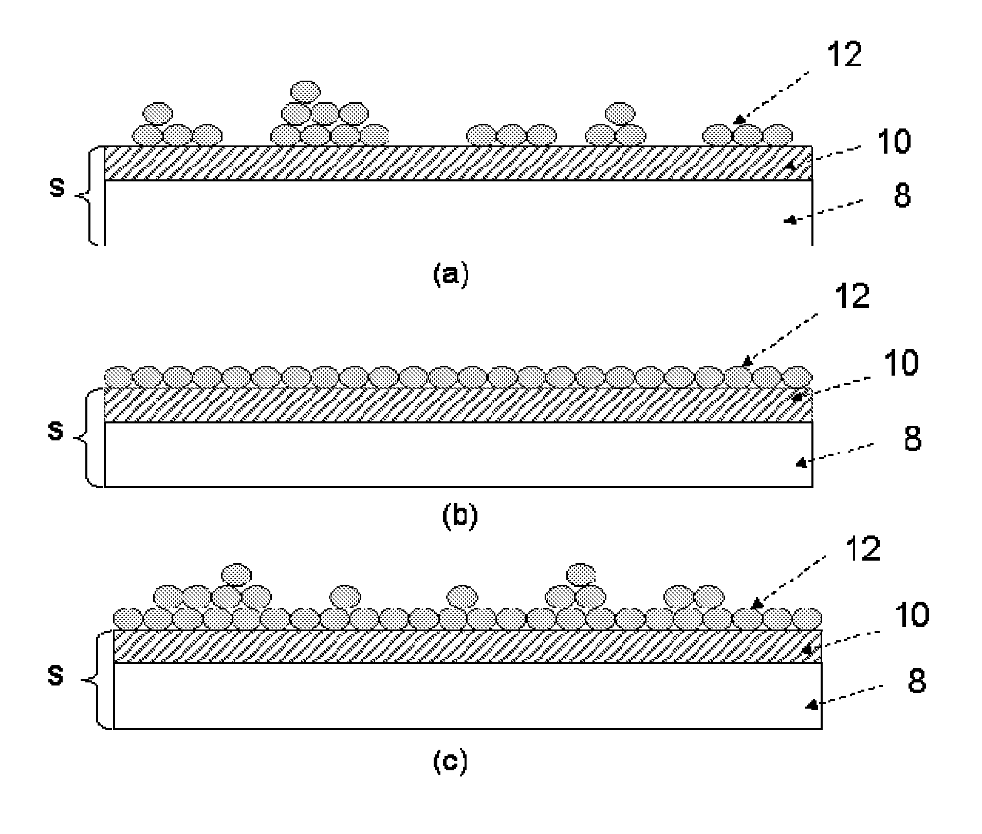
[0065]The invention will now further be described by a detailed description of several particular embodiments of the invention. It is clear that other embodiments of the invention can be configured according to the knowledge of persons skilled in the art without departing from the true spirit or technical teaching of the invention.

[0066]In the following detailed description, numerous specific details are set forth in order to provide a thorough understanding of the invention and how it may be practiced in particular embodiments. However it will be understood that the present invention may be practiced without these specific details. In other instances, well-known methods, procedures and techniques have not been described in detail, so as not to obscure the present invention. While the present invention will be described with respect to particular embodiments and with reference to certain drawings, the reference is not limited hereto. The drawings included and described herein are sc...


PUM


Abstract

A method for introducing species into a strained semiconductor layer comprising: providing a substrate comprising a first region comprising an exposed strained semiconductor layer, loading the substrate in a reaction chamber, then forming a conformal first species containing-layer by vapor phase deposition (VPD) at least on the exposed strained semiconductor layer, and thereafter performing a thermal treatment, thereby diffusing at least part of the first species from the first species-containing layer into the strained semiconductor layer and activating at least part of the diffused first species in the strained semiconductor layer.

Description

TECHNICAL FIELD OF THE INVENTION[0001]The invention is related to semiconductor devices and methods of manufacturing semiconductor devices. Particularly, the invention is related to methods for doping semiconductor structures and the semiconductor devices obtained thereof.BACKGROUND OF THE INVENTION[0002]Strained-silicon technology is a promising route to enhance metal-oxide-semiconductor field-effect transistor (MOSFET) performance due to improved carrier transport properties.[0003]In particular, biaxially-strained silicon on insulator substrate (abbreviated SSOI) is a promising source of strain engineering for the future CMOS technology nodes. The tensile stress in the Si layer results in an increased carrier mobility with respect to unstrained SOI. This in turn results in an enhanced drive current.[0004]As the scaling of strained-Si MOSFETs continues, the performance enhancement may become susceptible to degradation during processing, particularly from ion implantation and therma...

Claims


Application Information

Patent Timeline
Patent Type & Authority Applications(United States)
IPC IPC(8): H01L29/78H01L21/22H01L29/12
CPCH01L21/2254H01L21/2256H01L29/7842H01L29/66795H01L29/1054H01L29/66803
Inventor LOO, ROGERLEYS, FREDERIKCAYMAX, MATTY
Owner INTERUNIVERSITAIR MICRO ELECTRONICS CENT (IMEC VZW)
Why Eureka
Try Eureka