

Active matrix substrate, display panel, display device, and electronic apparatus
a technology of active matrix substrate and display panel, which is applied in the direction of semiconductor devices, instruments, optics, etc., can solve the problems of large proportion of manufacturing costs, difficult integration, and relatively high cost of data driving integrated circuit chips, and achieve the reduction of the load of the plurality of storage capacitor lines, preventing crosstalk, and sufficient storage capacitance
- Summary
- Abstract
- Description
- Claims
- Application Information
AI Technical Summary
Benefits of technology
Problems solved by technology
Method used
Image

Examples
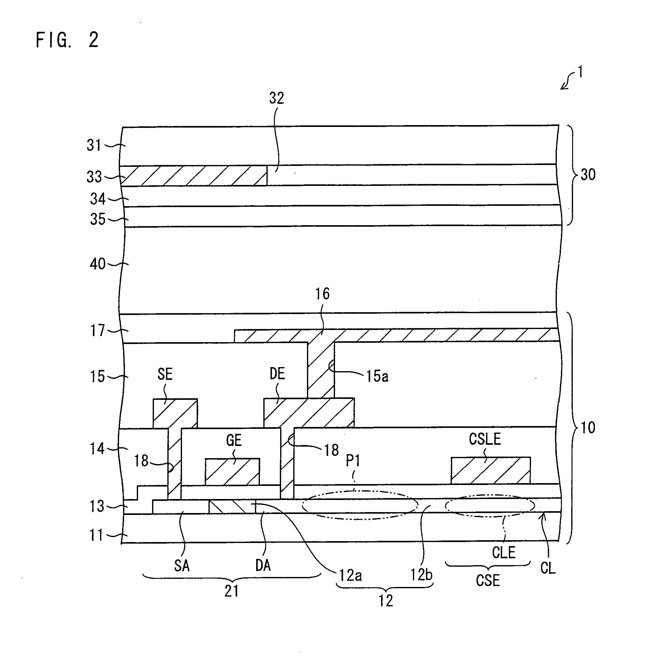
embodiment 1
[0069]The following describes an embodiment of the present invention, with reference to FIGS. 1 through 3.
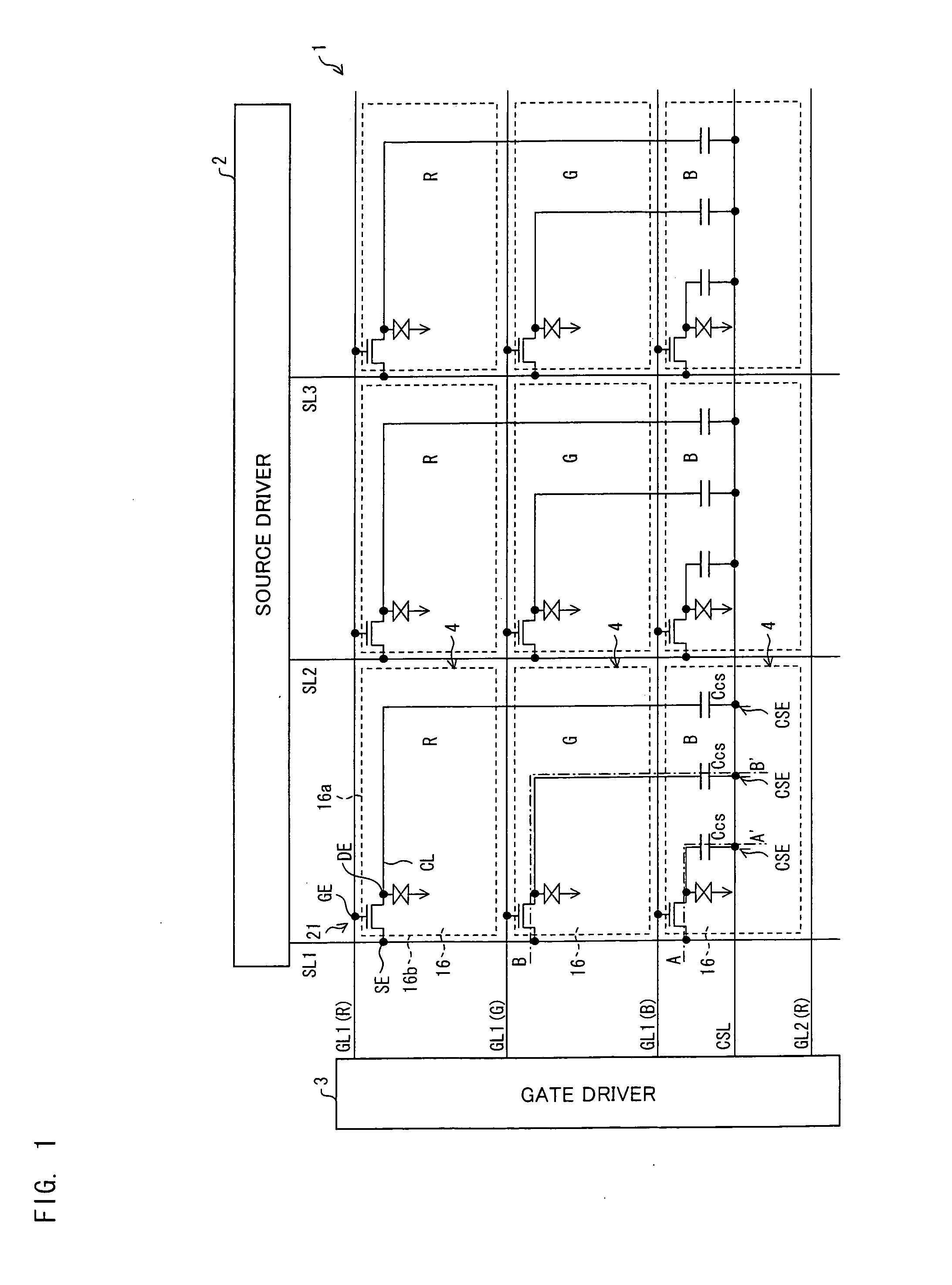
[0070]FIG. 1 is an equivalent circuit diagram of a liquid crystal panel included in a liquid crystal display device of the present embodiment.
[0071]For convenience of explanation, it is assumed that a direction in which gate lines extend is regarded as a row direction in the following descriptions. Note however that, the gate lines can extend either in a lateral direction or in a longitudinal direction when a liquid crystal display device including (i) a liquid crystal panel of the present embodiment or (ii) an active matrix substrate of the present embodiment included in the liquid crystal panel is actually used.
[0072]According to the present embodiment, the active matrix substrate is provided as a lower substrate (i.e., a substrate provided on backside) and a counter substrate is provided as an upper substrate (i.e., a substrate provided on viewer side). However, the present e...
embodiment 2
[0147]The following describes another embodiment of the present invention with reference to FIGS. 4 and 5. Note that, in the present embodiment, only differences from Embodiment 1 are described. Further, same reference numerals are given to components which have functions identical to those in Embodiment 1 and descriptions regarding such components are omitted.
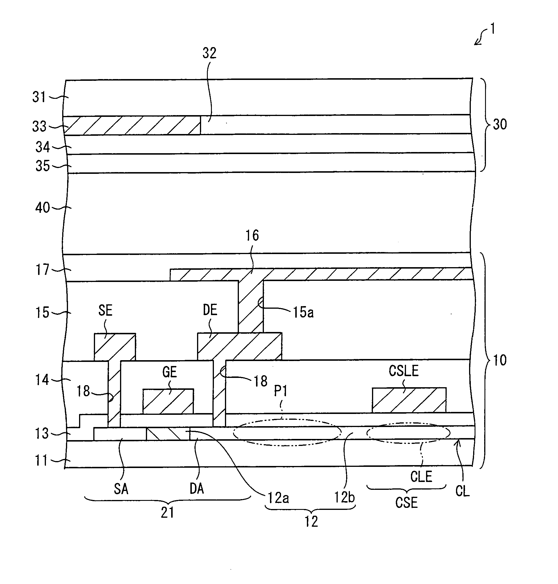
[0148]FIG. 4 is an equivalent circuit diagram illustrating a liquid crystal panel 1 included in the liquid crystal display device of the present embodiment. FIG. 5 is a cross-sectional view schematically illustrating a configuration of the liquid crystal panel 1 taken along the line C-C′ in FIG. 4.
[0149]The liquid crystal panel 1 shown in FIG. 4 is identical to that of Embodiment 1 except that the storage capacitor line CSL has (i) a main line CSL1 (trunk line) which is provided so as to extend in the row direction and (ii) a branch line CSL2 which is branched off from the main line CSL1 and extends in the column direction.
[01...
embodiment 3
[0157]The following describes yet another embodiment of the present invention with reference to FIG. 6. Note that, in the present embodiment, only differences from Embodiments 1 and 2 are described. Further, same reference numerals are given to components which have functions identical to those in Embodiments 1 and 2 and descriptions regarding such components are omitted.
[0158]FIG. 6 is an equivalent circuit diagram illustrating a liquid crystal panel 1 included in a liquid crystal display device of the present embodiment.
[0159]The liquid crystal panel 1 shown in FIG. 6 has configurations identical to those of Embodiment 1, except that (i) the liquid crystal panel 1 shown in FIG. 6 includes storage capacitor lines CSL11 (lateral lines) provided so as to extend in the row direction and storage capacitor lines CSL12 (longitudinal lines) provided so as to extend in the column direction and (ii) the storage capacitor lines CSL11 and the storage capacitor lines CSL are provided in a matr...
PUM
| Property | Measurement | Unit |
|---|---|---|
| drain area DA | aaaaa | aaaaa |
| voltages | aaaaa | aaaaa |
| data voltage | aaaaa | aaaaa |
Abstract
Description
Claims
Application Information