Memory component and memory device

a memory component and memory technology, applied in semiconductor devices, digital storage, instruments, etc., can solve the problems of insufficient resistance separation width of write resistance and erase resistance, and inability to maintain data. , to achieve the effect of improving erase characteristics, high resistance and facilitating maintenan

Inactive Publication Date: 2011-07-21
SONY CORP
View PDF8 Cites 13 Cited by
  • Summary
  • Abstract
  • Description
  • Claims
  • Application Information

AI Technical Summary

Benefits of technology

[0008]In view of the above situation, it is desirable to provide a memory component and a memory device, which can improve the maintenance characteristics of written data at low current and can lower a voltage necessary for an erase operation. It is also desirable to provide a memory component and a memory device, which can reduce the difference between resistance values in an erase state with respect to multiple write / erase operations.
[0014]Here, since the high resistance layer includes the layer that includes tellurium (Te) as the chief component among anion components, the metal element that has been diffused into the high resistance layer during the low-resistance state of the high resistance layer is stabilized to facilitate the maintenance in the low-resistance state. On the other hand, since tellurium (Te) has a weak bonding force with the metal element in comparison to an oxide or a silicon compound and the metal element which has been diffused into the inside of the high resistance layer is liable to move to the ion source layer, the erase characteristics are improved.
[0015]According to the memory component or memory device according to an embodiment of the present invention, since the high resistance layer in the memory layer includes a layer that includes tellurium (Te) as the chief component among anion components, the maintenance characteristics of the written data in a low-resistance state can be improved, and the low-voltage operation can be realized during the data erase. Further, it is possible to reduce the difference between the resistance values in the erase state with respect to multiple write / erase operations.

Problems solved by technology

However, the memory has the problem that if the rewrite current value is set to a low current equal to or less than 100 μA, the data maintenance characteristics deteriorate.
Also, due to insufficient characteristics during erase operation, a high voltage is necessary in erasing data.
Further, since the resistance value in an erase state tends to change toward a lower value with respect to multiple write / erase operations, the resistance separation width of write resistance and erase resistance becomes insufficient.

Method used


Image

  • Memory component and memory device
  • Memory component and memory device
  • Memory component and memory device

Examples


first embodiment

[0028](1) Memory component (memory component having a single-layer high resistance layer)

[0029](2) Memory device

Second Embodiment

[0030](1) Memory component (Memory component having two-layer high resistance layer)

example

First Embodiment

(Memory Component)

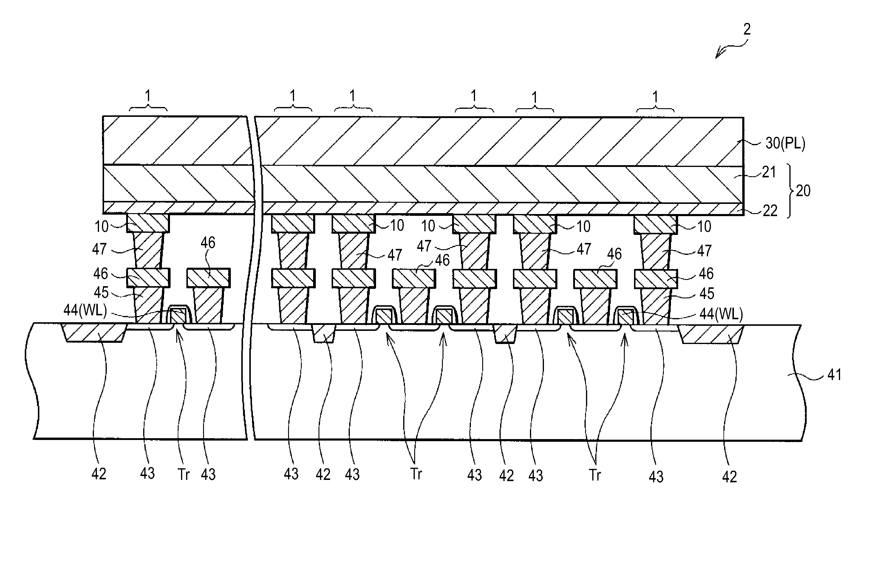
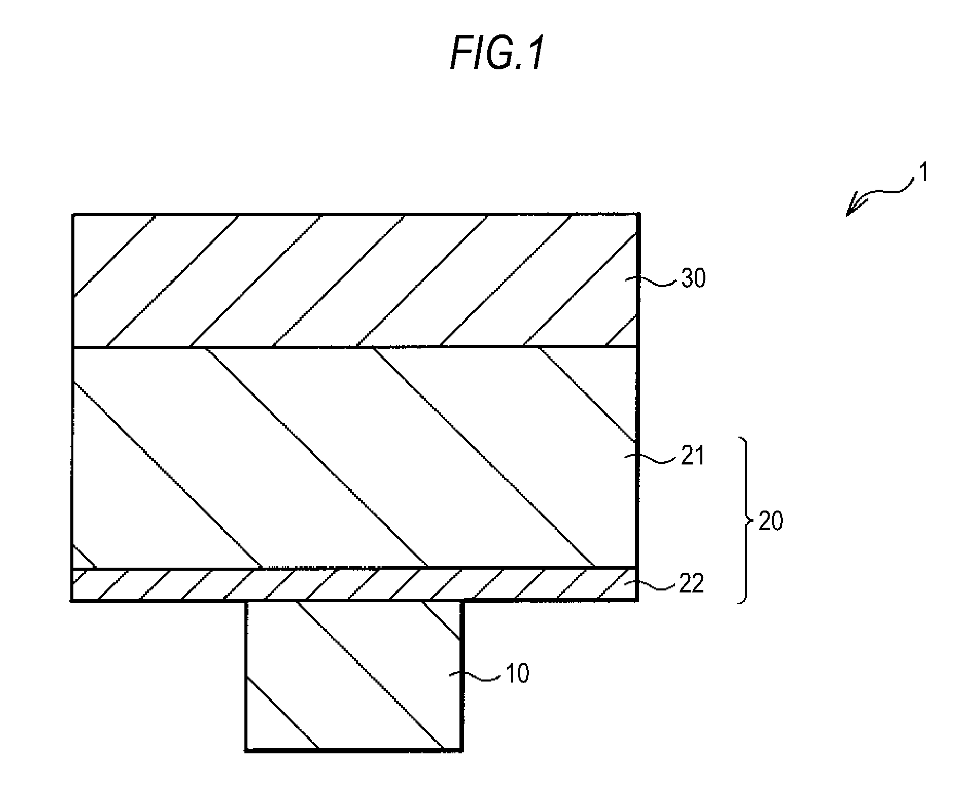
[0031]FIG. 1 is a cross-sectional view illustrating the configuration of a memory component 1 according to a first embodiment of the present invention. This memory component 1 includes a lower electrode (first electrode) 10, a memory layer 20, and an upper electrode (second electrode) 30 in this order.

[0032]The lower electrode 10, for example, as described later (FIG. 2), is formed on a silicon substrate 41 on which a CMOS (Complementary Metal Oxide Semiconductor) circuit is formed, and serves as a connection portion to the CMOS circuit portion. This lower electrode 10 is configured by an interconnection material used for a semiconductor process, for example, W (Tungsten), WN (Tungsten Nitride), Cu (Copper), Al (Aluminum), Mo (Molybdenum), Ta (Tantalum), silicide, or the like. In the case where the lower electrode 10 is made of a material such as copper (Cu) that has a possibility that ion conduction occurs in an electric field, the surface of the l...

second embodiment

[0073]FIG. 4 is a cross-sectional view illustrating the configuration of a memory component 3 according to a second embodiment of the present invention. Hereinafter, although other embodiments will be described, the same reference numerals are given to the same configuration portions as those according to the first embodiment, and the explanation thereof will be omitted. The memory component 3 includes a lower electrode (first electrode) 10, a memory layer 60, and an upper electrode (second electrode) 30 in this order.

[0074]The memory layer 60 includes anion source layer 61 that has the same composition as the ion source layer 21, and a high resistance layer 62. In this embodiment, the high resistance layer 62 has a double-layer structure of plural layers, for example, a first high resistance layer 62A and a second high resistance layer 62B. The first high resistance layer 62A and the second high resistance layer 62B function as barriers to the electric conduction, and have resistan...


PUM


Abstract

A memory component includes: a first electrode; a memory layer; and a second electrode in this order, wherein the memory layer includes a high resistance layer which includes tellurium (Te) as the chief component among anion components and is formed on the first electrode side; and an ion source layer which includes at least one kind of metal element and at least one kind of chalcogen element among tellurium (Te), sulfur (S) and selenium (Se) and is formed on the second electrode side.

Description

BACKGROUND OF THE INVENTION[0001]1. Field of the Invention[0002]The present invention relates to a memory component and a memory device, which store information in accordance with a change of the electrical characteristics of a memory layer that includes an ion source layer and a high resistance layer.[0003]2. Description of the Related Art[0004]As semiconductor nonvolatile memories for data storage, NOR type or NAND type flash memories are generally used. According to these semiconductor nonvolatile memories, however, a large voltage is necessary for write and erase operations, and the number of electrons that are injected into a floating gate is limited causing a limit on the miniaturization of the memory.[0005]Recently, resistance change type memories, such as ReRAM (Resistance Random Access Memory), PMC (Programmable Metallization Cell), or the like, have been proposed as next-generation nonvolatile memories that can overcome the limit on miniaturization (for example, Nature Mat...

Claims


Application Information

Patent Timeline
Patent Type & Authority Applications(United States)
IPC IPC(8): H01L45/00
CPCG11C13/0007G11C2213/51G11C2213/56H01L27/2436H01L27/2472H01L45/085H01L45/143H01L45/1266H01L45/141H01L45/144H01L45/1625H01L45/142H01L45/1233H10B63/30H10B63/82H10N70/245H10N70/826H10N70/8416H10N70/882H10N70/8828H10N70/026H10N70/231H10N70/8825H10N70/8822
Inventor YASUDA, SHUICHIROARATANI, KATSUHISAOHBA, KAZUHIROSEI, HIROAKI
Owner SONY CORP
Why Eureka
Try Eureka