Differential logic circuit, frequency divider, and frequency synthesizer

a logic circuit and frequency divider technology, applied in logic circuits, oscillators, pulse techniques, etc., can solve the problem that the current flow through the current source cannot be greatly varied

Inactive Publication Date: 2011-07-28
RENESAS ELECTRONICS CORP
View PDF11 Cites 3 Cited by
  • Summary
  • Abstract
  • Description
  • Claims
  • Application Information

AI Technical Summary

Benefits of technology

However, a rise speed at the data output terminal Q or Qb is determined by the resistance value of the load resistance R11 or R12, an element connected to the output terminal, and a wiring parasitic capacitance. Thus, the rise speed does not vary even if the current that is flown through the current source 930 is varied. That is, when the traditional differential latch circuit as described in FIG. 4 is used, the fixed load resistances are used, so that the rise speed at the data output terminal Q or Qb does not vary even if the magnitude of the current that is flown through the current source is adjusted. Thus, a maximum toggle frequency variable range of the differential latch circuit is small. When the current that is flown through the current source is varied, a direct-current output voltage of the differential latch circuit is varied, thereby affecting an operation in the next stage. Thus, the current that is flown through the current source cannot be greatly varied. Accordingly, in the frequency divider circuit using the traditional differential latch circuit, the adjustment range of a maximum operable frequency of the frequency divider circuit implemented by adjustment of the circuit current is narrow. The differential latch circuit and the frequency divider as described above cannot accommodate a frequency synthesizer used in terminals for mobile communication in which lower power consumption, bandwidth expansion, and multiple bands in recent years have been promoted. A differential latch circuit and a frequency divider capable of accommodating a wide frequency range and implementing power consumption that is as low as possible in any frequency band is desired.
The meritorious effects of the present invention are summarized as follows. According to the differential logic circuit and / or the frequency divider of the present invention, the load of the load circuit is controlled such that the direct-current output voltage of the differential output terminals holds a constant value, irrespective of the magnitude of the current that is flown through the current source circuit. Thus, by controlling current that is flown through the current source circuit, an operating current can be varied in a wide range. Accordingly, a differential logic circuit and a frequency divider with a high-speed operation and low power consumption according to an operation speed required for the circuit can be obtained.

Problems solved by technology

Thus, the current that is flown through the current source cannot be greatly varied.
The differential latch circuit and the frequency divider as described above cannot accommodate a frequency synthesizer used in terminals for mobile communication in which lower power consumption, bandwidth expansion, and multiple bands in recent years have been promoted.

Method used


Image

  • Differential logic circuit, frequency divider, and frequency synthesizer
  • Differential logic circuit, frequency divider, and frequency synthesizer
  • Differential logic circuit, frequency divider, and frequency synthesizer

Examples


first exemplary embodiment

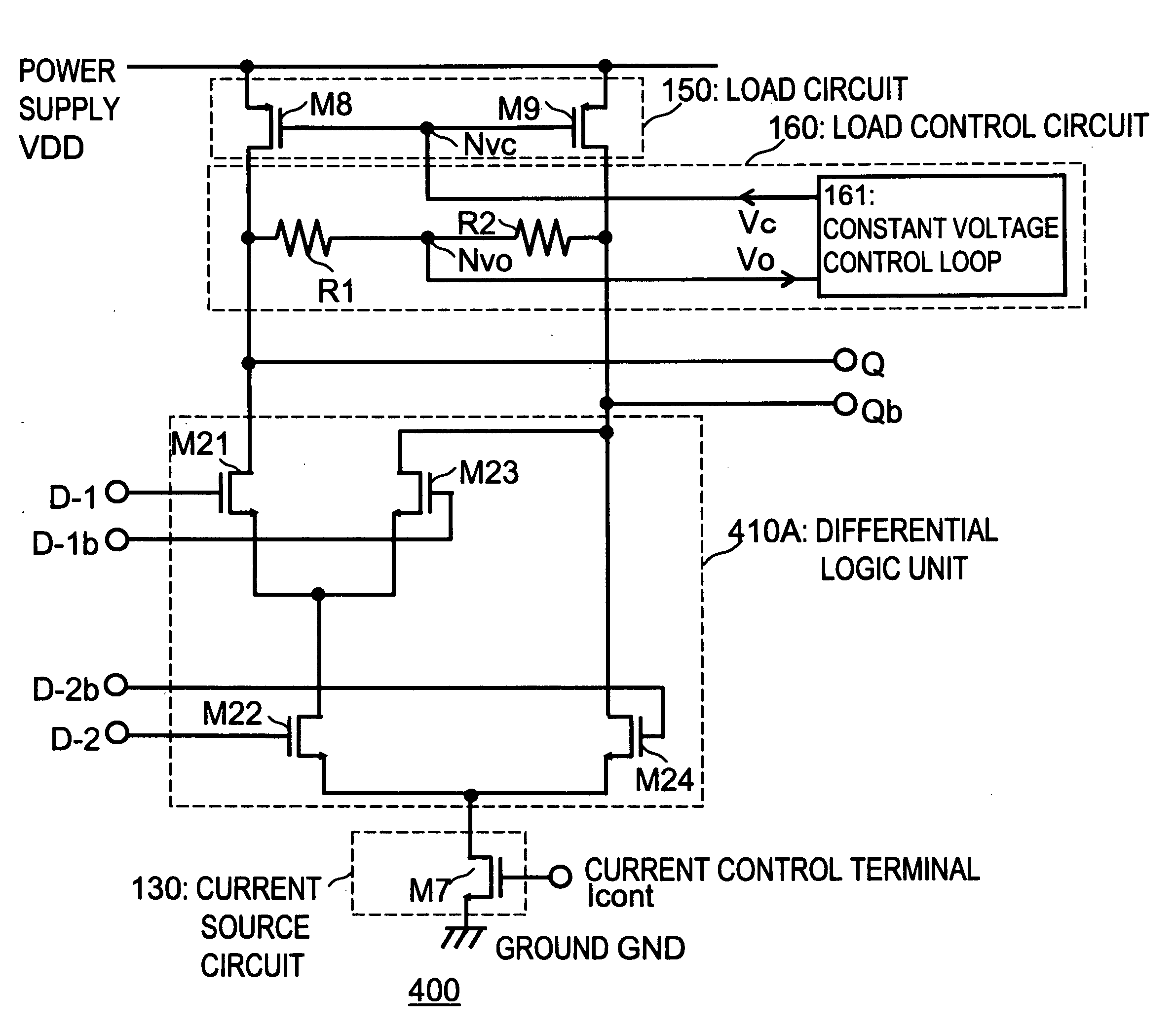
FIG. 6 is a circuit block diagram of a differential latch circuit 100, which is a differential logic circuit according to a first example. The differential logic circuit includes a current source circuit 130 that supplies a power supply to the differential logic circuit, a differential logic unit 410 that implements a desired differential logic, a load circuit 150, and a load control circuit 160.

The current source circuit 130 includes an N-channel MOS transistor M7 with a gate thereof connected to a current control terminal and a source thereof connected to the ground GND, and supplies a power supply current (operating current) of the differential logic unit 410. It is arranged that the operating current output from a drain of the N-channel MOS transistor M7 can be controlled by a voltage of a current control signal Icont received from the current control terminal.

A circuit that implements logic of the differential latch circuit 100 is provided at the differential logic unit 410. In...

second exemplary embodiment

The internal circuit configuration of the load control circuit (constant voltage control loop) in FIG. 7 described in the first example is a most preferable configuration example. The load control circuit is not limited to the configuration in FIG. 7 using the current output type differential amplifier circuit 170. The load control circuit may use a more common voltage output type differential amplifier circuit. FIG. 10 is a circuit block diagram of a load control circuit 160A in a second example. FIG. 10 describes a load circuit 150 as well, in addition to the load control circuit 160A in the second example. Referring to FIG. 10, a voltage output type differential amplifier circuit 170A is a voltage output type operational amplifier circuit in which a potential difference between a signal applied to a non-inverted signal input terminal thereof and a signal applied to an inverted signal input terminal thereof is infinitely amplified to be large and is then output from a voltage outp...

third exemplary embodiment

FIG. 11 is a circuit block diagram of a ½ frequency divider according to a third example. A ½ frequency divider 190 is formed of two differential latch circuits 100-1 and 100-2 in the first example. A load control circuit 160 is provided in common to the two differential latch circuits 100-1 and 100-2. Gates of active loads M8 and M9 in the differential latch circuit 100-1 and gates of active loads M18 and M19 in the differential latch circuit 100-2 are connected in common to a control voltage output terminal of the load control circuit 160, for supply of a control voltage Vc. Resistances R1 and R2 of the load control circuit 160 are connected to output terminals Q and Qb of the differential latch circuit 100-2.

A non-inverted clock signal Ck and an inverted clock signal Ckb supplied from differential clock signal input terminals Ck and Ckb are connected in common to switch circuits (M5 and M6, and M15 and M16) of the differential latch circuits 100-1 and 100-2. The clock signals con...


PUM


Abstract

A differential logic circuit includes: a differential logic unit which receives a plurality of logic signals, performs a logic operation, and outputs a result of the logic operation from a pair of differential signal output terminals thereof; and a current source circuit which supplies current to the differential logic unit and which controls a magnitude of the current. The differential logic circuit further includes: a load circuit connected to the differential signal output terminals; and a load control circuit which is connected to the load circuit and controls a load of the load circuit such that a direct-current output voltage of the pair of differential signal output terminals is constant.

Description

TECHNICAL FIELDReference to Related ApplicationThis application is based upon and claims the benefit of the priority of Japanese patent application No. 2010-15219, filed on Jan. 27, 2010, the disclosure of which is incorporated herein in its entirety by reference thereto. The present invention relates to a differential logic circuit, a frequency divider, and a frequency synthesizer. More specifically, the invention relates to a differential latch circuit of which an operating current can be controlled, a frequency divider and a frequency synthesizer both using the differential latch circuit.BACKGROUNDFrequency synthesizers are widely used in communication devices, mobile communication terminals, and high-frequency integrated circuits used for the mobile communication terminals in order to generate a high-frequency communication carrier. FIG. 1 is a block diagram showing a configuration of a common frequency synthesizer. The frequency synthesizer shown in FIG. 1 is a PLL frequency sy...

Claims


Application Information

Patent Timeline
IPC IPC(8): H03K19/094H03K23/00
CPCH03K23/662H03K19/01855
Inventor WANG, JIANQIN
Owner RENESAS ELECTRONICS CORP
Why Eureka
Try Eureka