Method of manufacturing a substrate for a mask blank, method of manufacturing a mask blank, method of manufacturing a transfer mask , and method of manufacturing a semiconductor device

a technology of mask blanks and substrates, which is applied in the direction of manufacturing tools, photomechanical equipment, instruments, etc., can solve the problems of increasing the demand for further miniaturization of semiconductor devices, the accuracy of transfer patterns on the transfer target, and the focal depth of exposure apparatuses becoming extremely small, so as to accurately estimate the main surface shape of the transparent substrate, accurately estimate the displacement of the transfer pattern, accurate estimate

Active Publication Date: 2011-08-04
HOYA CORP
View PDF5 Cites 12 Cited by
  • Summary
  • Abstract
  • Description
  • Claims
  • Application Information

AI Technical Summary

Benefits of technology

[0037]By taking into account, in a simulation, a twist deformation being a deformation which acts in a direction to correct torsion of a transparent substrate when the transparent substrate is chucked in an exposure apparatus, it is possible to more accurately estimate a main surface shape of the transparent substrate when it is chucked in the exposure apparatus. As a consequence, it is possible to select a transparent substrate which is suitable as a mask blank substrate for a transfer mask for use in an exposure apparatus using the immersion exposure technique. Since the main surface shape after chucking can be accurately estimated, it is possible to accurately estimate displacement of a transfer pattern with respect to a reference plane before and after the transfer mask is chucked, and thus to correct a design pattern in consideration of such displacement of the transfer pattern to thereby produce the transfer mask.
[0038]Further, by taking into account, in a simulation, a twist deformation being a deformation which acts in a direction to correct torsion of a mas

Problems solved by technology

However, demand for further miniaturization of semiconductor devices is increasing more and more and, with the introduction of the immersion exposure technique, hyper-NA, i.e. NA>1, has been achieved so that the focal depth of exposure apparatuses is becoming extremely small.
Particularly in the case of a transfer mask applied with the double patterning technique, if the estimation accuracy of a substrate shape change before and after chucking is low, the estimation accuracy of the displacement of the position of a transfer pattern with respect to the reference plane on the mask stage due to the substrate shape change is also lowered so that a serious problem arises on the transfer accuracy of the transfer pattern onto a transfer target (a

Method used


Image

  • Method of manufacturing a substrate for a mask blank, method of manufacturing a mask blank, method of manufacturing a transfer mask , and method of manufacturing a semiconductor device
  • Method of manufacturing a substrate for a mask blank, method of manufacturing a mask blank, method of manufacturing a transfer mask , and method of manufacturing a semiconductor device
  • Method of manufacturing a substrate for a mask blank, method of manufacturing a mask blank, method of manufacturing a transfer mask , and method of manufacturing a semiconductor device

Examples


example

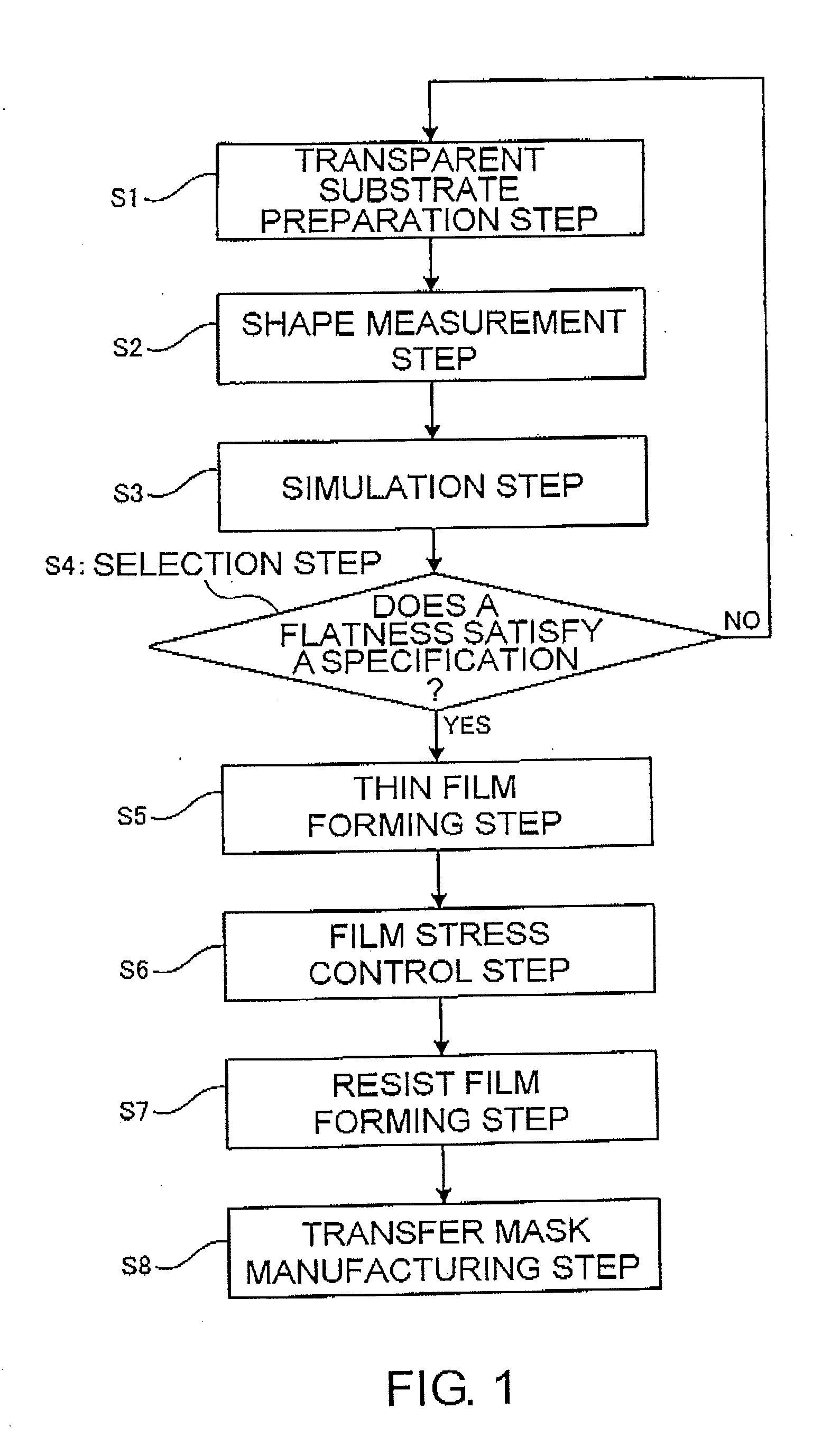
[0100]Hereinbelow, transfer mask manufacturing steps including mask blank substrate manufacturing steps and mask blank manufacturing steps will be described in detail with reference to an Example.

[0101](I) Transparent Substrate Preparation Step

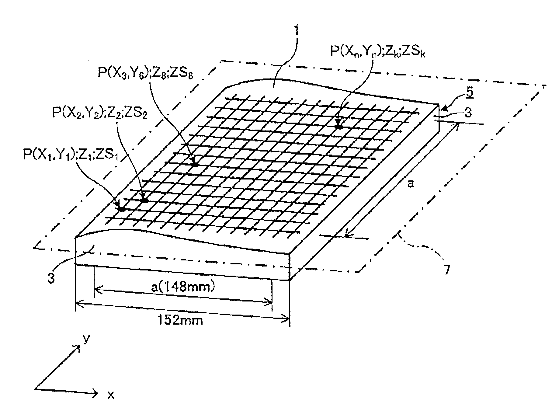
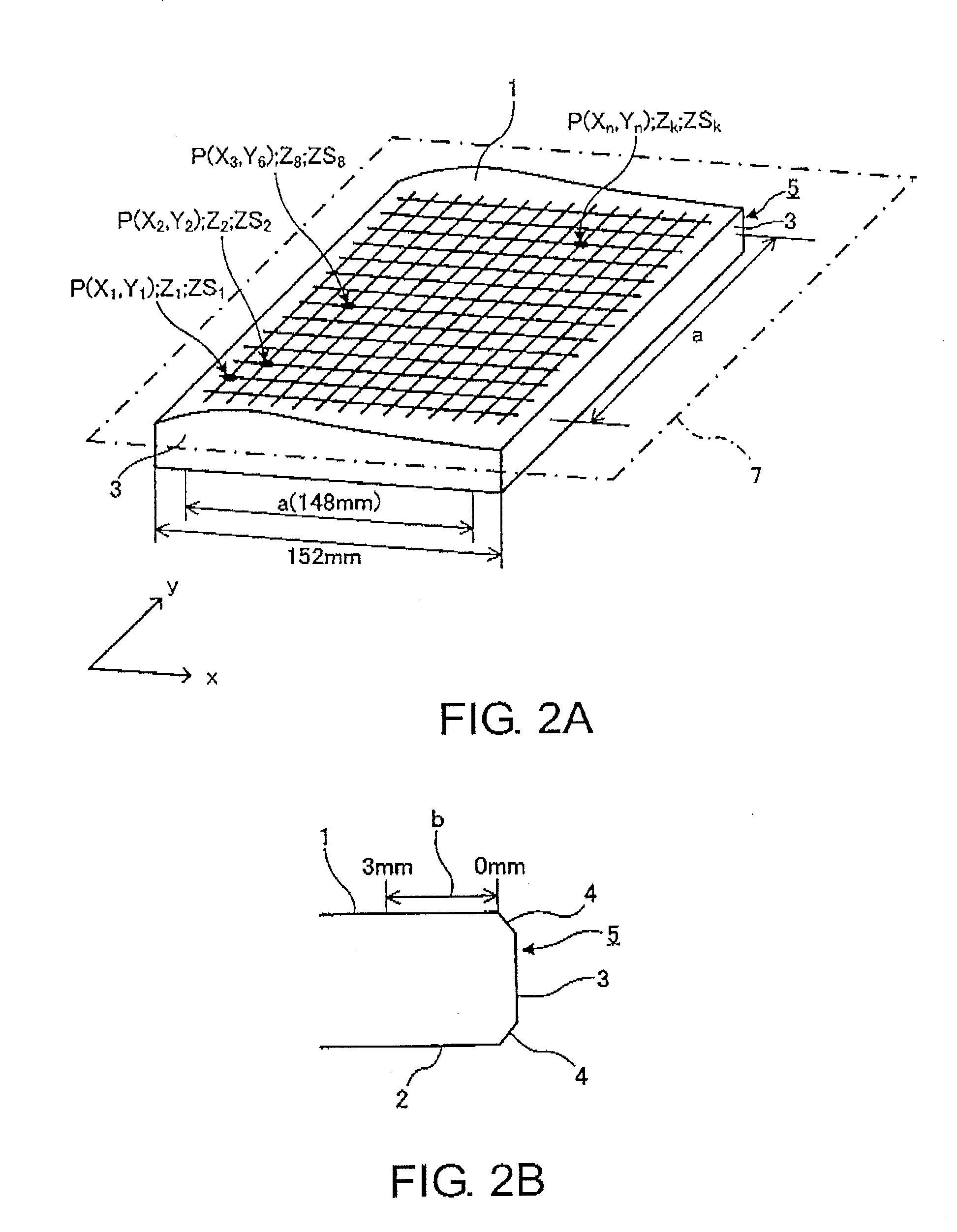
[0102]Main surfaces of square transparent plates (synthetic quartz glass plates) were precision-polished and cleaned, thereby preparing 20 transparent substrates (about 152 mm×about 152 mm×6.35 mm).

[0103](II) Shape Measurement Step

[0104]With respect to each of the 20 transparent substrates, using a flatness measuring apparatus (UltraFlat200M manufactured by Corning Tropel Corporation) utilizing an optical interferometer, information of a before-chucking main surface shape (height information from a focal plane (virtual absolute plane) calculated by the method of least squares) was obtained at 256×256 measurement points in an actual measurement region (148 mm×148 mm) on the main surface (the main surface where a pattern-formation thin film was ...


PUM

PropertyMeasurementUnit
Lengthaaaaaaaaaa
Lengthaaaaaaaaaa
Lengthaaaaaaaaaa

Abstract

In a simulation step, based on information of a main surface shape of a transparent substrate and shape information of a mask stage of an exposure apparatus and using a deflection differential equation taking into account a twist deformation, height information at a plurality of measurement points is obtained by simulating a state where the transparent substrate is set in the exposure apparatus. Based on the height information obtained through the simulation, a flatness of the transparent substrate when it is set in the exposure apparatus is calculated in a flatness calculation step. Then, by judging in a selection step whether or not the calculated flatness satisfies a specification, the transparent substrate whose flatness satisfies the specification is used as a substrate for a mask blank.

Description

[0001]This application is based upon and claims the benefit of priority from Japanese Patent Application No. 2010-018283, filed on Jan. 29, 2010, and Japanese Patent Application No. 2010-277846, filed on Dec. 14, 2010, the disclosures of which are incorporated herein in their entirety by reference.TECHNICAL FIELD[0002]This invention relates to a method of manufacturing a substrate for a mask blank (hereinafter referred to as a “mask blank substrate”), a method of manufacturing a mask blank, a method of manufacturing a transfer mask, and a method of manufacturing a semiconductor device.BACKGROUND ART[0003]With the miniaturization of semiconductor devices in recent years, the reduction in wavelength of exposure light for use in photolithography has been proceeding. In the advanced technical field of transmission photolithography, ArF excimer laser light (wavelength: 193 nm) with a wavelength of 200 nm or less is used as exposure light. However, demand for further miniaturization has b...

Claims


Application Information

Patent Timeline
IPC IPC(8): G03F1/00G03F7/20C03B20/00C03C19/00G03F1/50G03F1/60
CPCC03C19/00C03B20/00G03F7/20G03F1/50G03F1/60G03F1/00Y02P40/57G03F7/70783G03F1/84G03F1/72H01L21/0274H01L21/0337
Inventor TANABE, MASARU
Owner HOYA CORP
Why Eureka
Try Eureka