[0014]However, the inventors have also realised that the relationship of a measured mass distribution to the
characteristic distribution corresponding to a mass
fingerprint and the location of individual measurements relative to a
characteristic distribution can be indicative of properties of the device, i.e. properties of the element fabricated by the process having the
fingerprint. In other words, a comparison of a measured mass change distribution for a current batch of wafers with a predetermined characteristic mass change distribution for a process may yield useful information about the process that may otherwise be difficult to detect. For example, mass measurements may be related to thickness, layer uniformity,
stoichiometry, stress and
refractive index. During fabrication, there will be variations in the process and for each of these parameters there will be a corresponding
characteristic distribution. The inventors have understood that all of these distributions can be captured by measuring only the distribution of the mass
fingerprint for the process. Moreover, if an
empirical relationship between one or more parameters and the mass fingerprint is determined, it may be possible to detect behaviour of the one or more parameters from the measured mass fingerprint distribution. It may thus be possible to link the behaviour of the measured mass change distribution to a certain effect whereby adjustment of the process is targeted at corrected for that effect. Certain behaviour of the measured mass change distribution may indicate the onset of an error. In one embodiment this aspect of the invention may provide a means of detecting problems in the
system which are flagged by changes in parameters that can only be measured directly in a destructive manner. The determined
empirical relationship permits the evolution of a distribution of non-destructive measurements of mass change to be used to indicate behaviour of a parameter that can only be measured destructively. For example, it is not possible to perform non-destructive measurements of stress on thin SiN films formed on product wafers. However, a previously established empirical relationship between a
stress distribution and its corresponding characteristic mass change may permit changes in stress to be detected as changes in a measured mass change distribution.
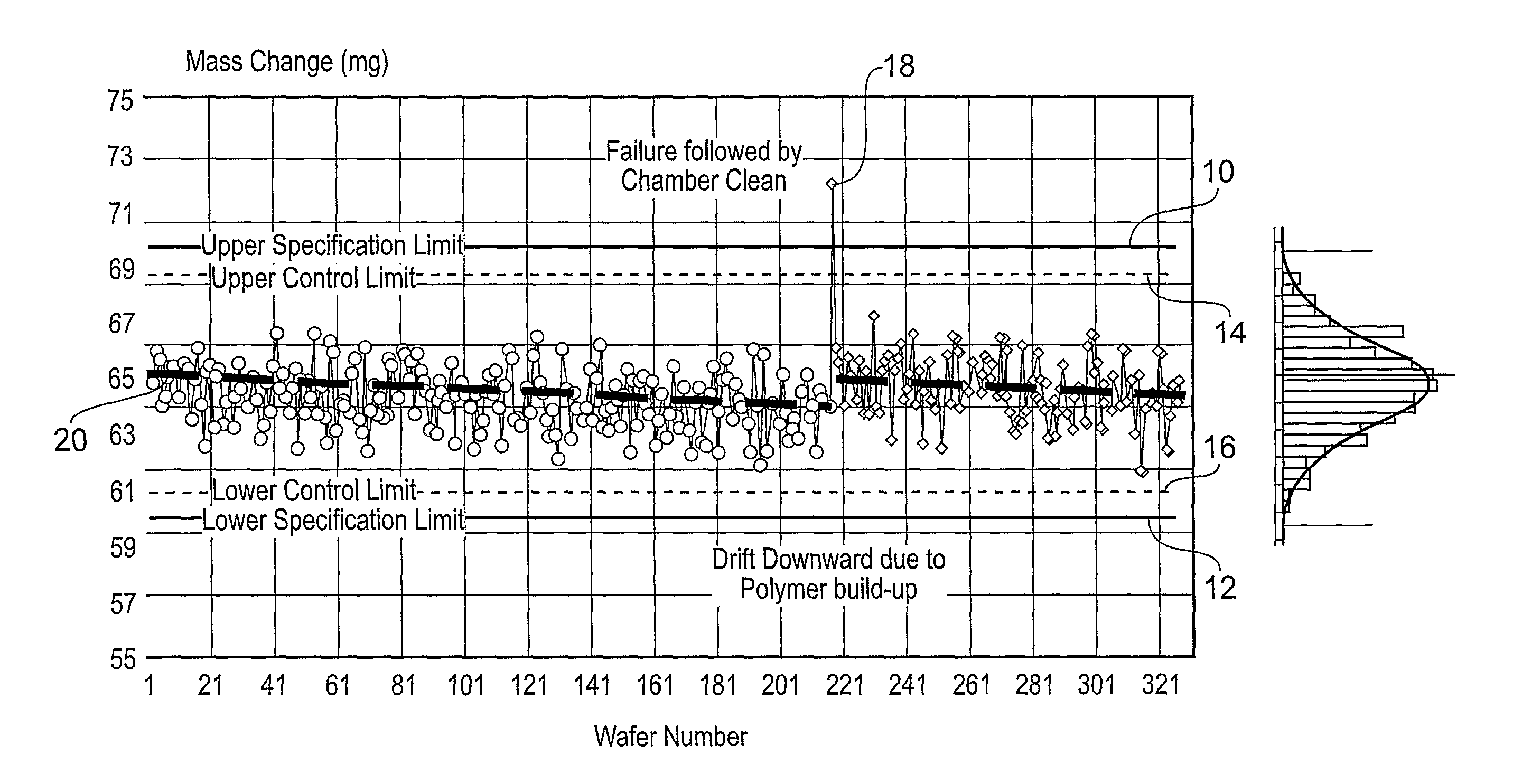
[0016]A particular
advantage of the proposed method is that it may permit adjustments to the process to be determined and implemented before a predetermined
process control limit is breached. In other words, the method may be used to identify
mass measurement patterns which fall within the
control limits of a given distribution but which indicate the onset of problems in the process.
[0017]Alternatively or additionally, the location of an individual mass change measurement (e.g. for a single semiconductor wafer) within a current mass change distribution may provide information about that wafer. Herein a current mass change distribution may be a mass change distribution consisting of measured mass changes of a plurality of wafers subjected to the process before the individual mass change measurement is taken. Whereas in known SPC techniques measurements of one or more semiconductors wafers are compared with static
control limits, e.g. set in fixed positions relative to a characteristic distribution, in the invention the relative position of a measurement within a distribution is detected. This relative position may be indicative of problems with that individual wafer. Such problems may be independent of problems that affect the behaviour of the distribution as a whole. The invention may thus facilitate detection of problems that would otherwise go undetected. For example, in a situation where the mean of a distribution slips below the characteristic mean, a high
outlier in the
current distribution may fall within the
control limits of the characteristic distribution and hence be deemed acceptable whereas a comparison with the
current distribution may indicate that a problem with that wafer has occurred.
[0020]According to one aspect of the invention, there may be provided a method of
statistical process control (SPC) including: obtaining a characteristic mass change distribution for a
semiconductor wafer fabrication process; measuring a change in mass of a plurality of semiconductor wafers subjected to the process; comparing the shape of a measured mass change distribution consisting of the measured mass changes of the plurality of semiconductor wafers with the shape of the characteristic mass change distribution to monitor the process. This aspect may provide a way of monitoring the effectiveness of any fabrication process step by comparing a ‘current’, i.e. recently obtained, distribution with a characteristic, e.g. ideal, distribution to identify problems in the process. For example, the mean of the current distribution may stray from the mean of the characteristic distribution. This can be an indicator that the process is not performing efficiently and appropriate
remedial action can be undertaken. An
advantage of the method is that the
remedial action can be taken in an efficient manner, i.e. before an unsatisfactory wafer is produced by the process but not so often as to unnecessarily disrupt the fabrication process.
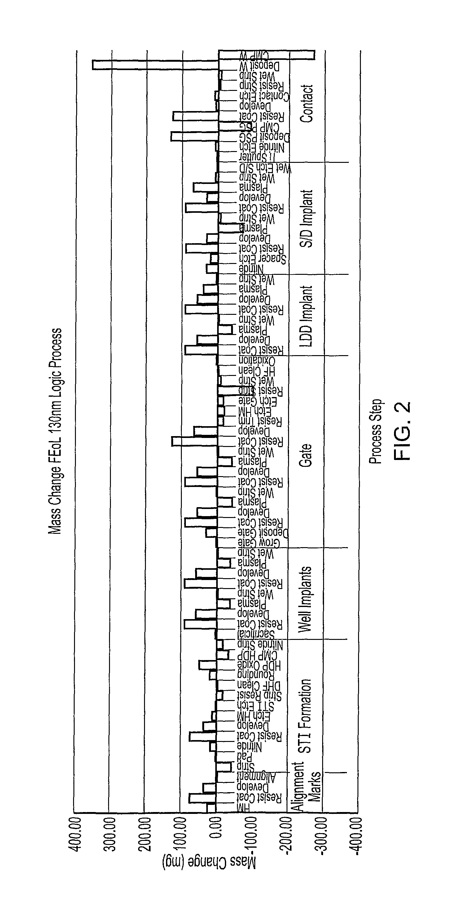
[0029]The characteristic mass change distribution may result from a detailed investigation of a process before that process is incorporated into fabrication of product wafers. The investigation may involve obtaining a correlation between variations in the process and mass change. During the investigation, the variations in the process may be definitively measured e.g. using destructive techniques not suitable for product wafers. In this way the characteristic mass change distribution can be used effectively as a means to match non-destructive mass change measurements (i.e. measurements suitable for use on product wafers) with properties of the process that cannot be determined directly in a non-destructive manner. However, obtaining such links is not essential: changes in the measured mass change distribution may be linked directly through experience with problems with the process.
[0035]In a further development, the method of the invention may include comparing the indication of the
control variable obtained via mass
metrology with information about the process, preferably information about the control variable, obtained by another (non-mass) metrology measurement. The other metrology measurement may also be non-destructive so that it can be used effectively on product wafers. Using the mass metrology technique in combination with another metrology output may enable anomalies or errors to be picked up that would otherwise remain undetected. For example,
ellipsometry can be used to determine the thickness and uniformity of certain types of film. In one embodiment,
ellipsometry data may show that a deposited film measured at a specific location (i.e. a flat area) is good, but the mass change measurement may not lie in the expected band, which may indicate that there is a problem at a location not measurable by
ellipsometry, i.e. there may be a problem with film coverage in a gap where device fabrication is taking place. Such problems may have gone undetected if ellipsometry was used alone.

