Array substrate of liquid crystal display device and repair method thereof

a liquid crystal display and array substrate technology, applied in semiconductor devices, instruments, optics, etc., can solve the problems of low quality display substrates, line defects of array substrates, scrapping of low-quality display substrates,

Inactive Publication Date: 2011-08-11
CENTURY DISPLAY (SHENZHEN) CO LTD
View PDF2 Cites 10 Cited by
  • Summary
  • Abstract
  • Description
  • Claims
  • Application Information

AI Technical Summary

Benefits of technology

[0011]It is therefore one of the objectives of the present invention to provide an array substrate of a liquid crystal display panel and a repair method ther

Problems solved by technology

It is to be noted that, in actual manufacturing, line defects often occur in the array substrate due to process unsteadiness or other factors, the line defects often refer to the defects of the scan lines or the defects of the data lines on the substrate.
When the line defects reduce the quality of the display, the low quality substrates of the display are scrapped.
Although the method above can repair the line defects, the laser repair method requires additional structure designs (e.g. the designs of the protrusions 21), which greatly increases the complexity of the pixel structure as well as the difficulty of the process of manufacturing.
Furthermore, other defects may be introduced during the method described above, e.g. contamination of the pixel electrode during the formation of the protrusions could occur, affecting the quality of the display of the panel.
Although such method is less complicated, the extension part 16 would generate a parasitic capacitance, which adversely affects the display quality.
Although such method can repair the scan line wit

Method used


Image

  • Array substrate of liquid crystal display device and repair method thereof
  • Array substrate of liquid crystal display device and repair method thereof
  • Array substrate of liquid crystal display device and repair method thereof

Examples


Embodiment Construction

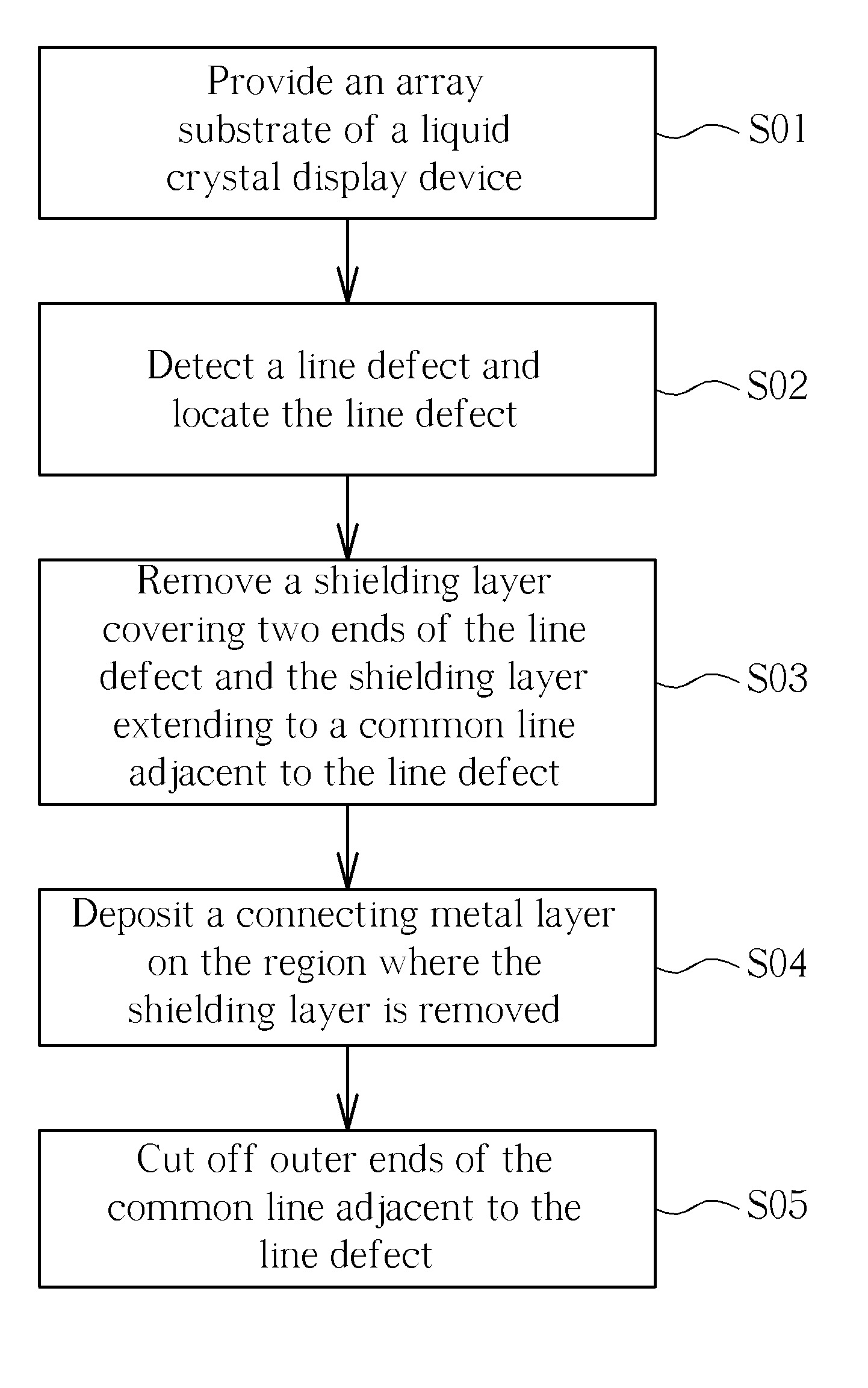
[0041]The methods and structures described in the following embodiments, not only repair the line defect of the data line or the scan line, but also design the signal transmitting wires to ensure the aperture ratio of the pixel.

[0042]FIG. 4 is a schematic line defect repair process flow diagram in accordance with the present invention. As illustrated in FIG. 4, the repair process includes the following steps. First, provide an array substrate of a liquid crystal display device (S01); then, detect a line defect and locate the line defect (S02). The detections may be executed by AOI machine or other methods / machines, e.g. a TESTER machine could detect, for detecting any line defect of the signal transmitting wires. The signal transmitting wires described above include a data line and a scan line. Then, locate the positions of the line defects at the data line or the scan line and remove a shielding layer covering two ends of the line defect and the shielding layer extending to a commo...


PUM


Abstract

A repair method for an array substrate of a liquid crystal display device includes, providing an array substrate for a liquid crystal display device, detecting a line defect of a signal transmitting wire and locating the line defect, performing a removal process to remove a shielding layer covering two ends of the line defect and the shielding layer extending to a common line adjacent to the line defect, performing a deposition process to deposit a connecting metal layer the region where the shielding layer is removed, and performing a cutting process to cut outer ends of the common line adjacent to the line defect to form a common line section. The signal transmitting wire forms an electrical circuit with the common line section.

Description

BACKGROUND OF THE INVENTION[0001]1. Field of the Invention[0002]The present invention relates to an array substrate of a liquid crystal display and a repair method thereof, and more particular, to an array substrate of the liquid crystal display device and a repair method thereof that repairs line defects.[0003]2. Description of the Prior Art[0004]Nowadays, because of many advantages, such as high display quality, good space utilization, low power consumption, and low radiation, the liquid crystal display device has become more and more popular. As the liquid crystal display technology advances, the liquid crystal display device has been widely employed in many fields. Generally, the liquid crystal display device includes an array substrate, a counter substrate and a liquid crystal layer sandwiched between the two substrates. The array substrate mainly includes a substrate, pixel structures arranged on the substrate in an array, a plurality of scan lines and a plurality of data line...

Claims


Application Information

Patent Timeline
IPC IPC(8): G02F1/1343H01L21/30
CPCG02F1/136259H01L27/124H01L21/76894G02F2001/136263G02F1/136263
Inventor CHENG, I-MINGBIAN, DE
Owner CENTURY DISPLAY (SHENZHEN) CO LTD
Why Eureka
Try Eureka