

Material for organic electronic device, and organic electronic device using same
a technology of electronic devices and materials, applied in the direction of organic chemistry, sustainable manufacturing/processing, final product manufacturing, etc., can solve the problems of difficult to produce an organic light emitting device with high efficiency and a long lifespan, and difficult to apply to an organic light emitting device requiring a high current, so as to improve the life time property of the device, reduce the driving voltage of the device, and improve the effect of light efficiency
- Summary
- Abstract
- Description
- Claims
- Application Information
AI Technical Summary
Benefits of technology
Problems solved by technology
Method used
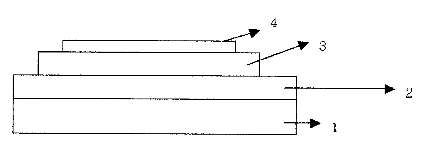
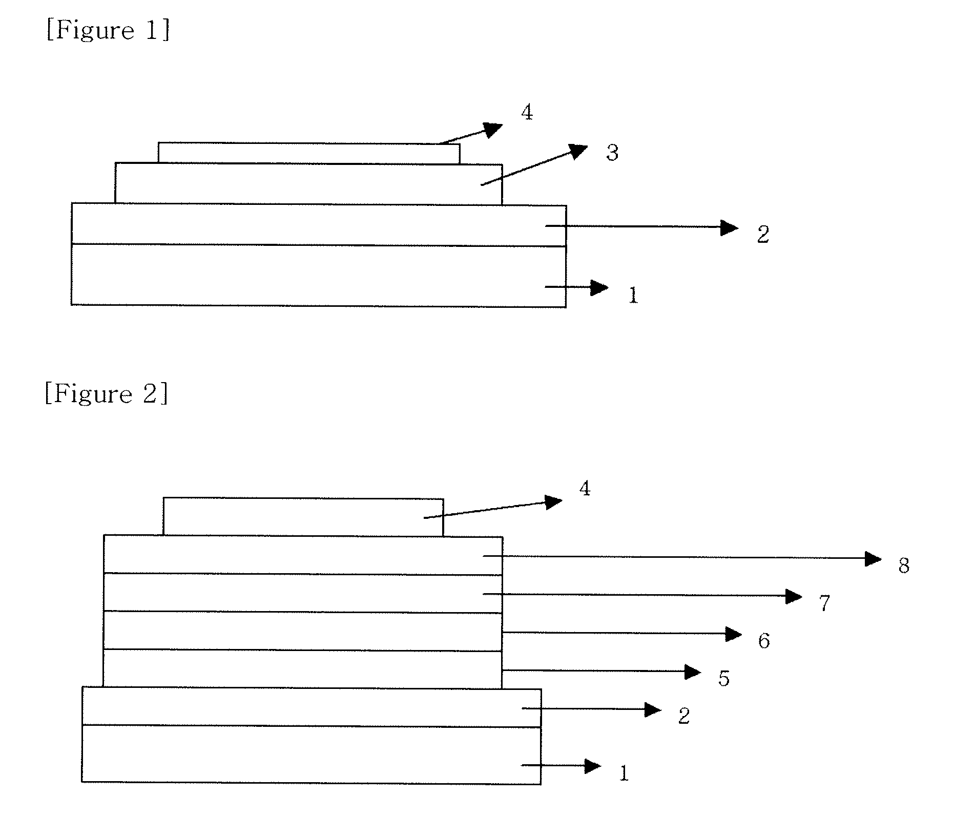
Image

Examples
synthesis example 1-b-no
Manufacturing of the Compound Represented by Formula 1-B-No
[0091]The compound 1-B, the aryl compound that was substituted with an excessive amount of iodine, 1 to 2 equivalents of Cu powder, and 3 to 6 equivalents of K2CO3 was added thereto, heated and agitated. The reactants were cooled to normal temperature, and extracted, distilled, purified, and dried with the organic solvent to manufacture the 1-B-No compound, the specific compound synthesized 1-B-1, and the results thereof are described in Table 1-B-No.
synthesis example 1-b-1
Manufacturing of the Compound Represented by Formula 1-B-1
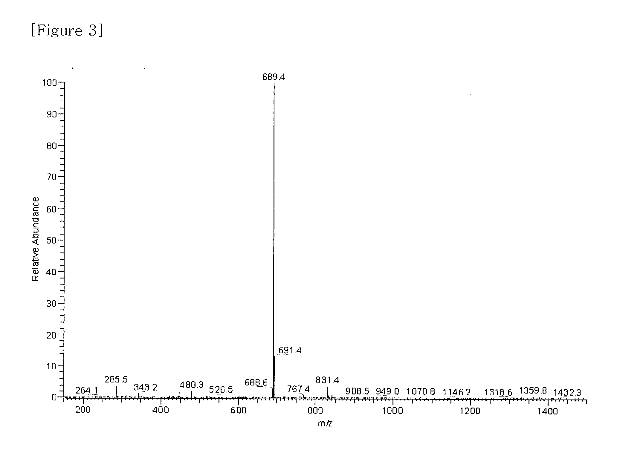
[0092]The compound 1-B (10.0 g, 33.8 mmol), 120 ml of iodobenzene, 2 equivalents of Cu powder (4.3 g, 67.6 mmol), and 3 equivalents of K2CO3 (14.0 g, 101.4 mmol) were added thereto, heated and agitated for 12 hours. The reactants were cooled to normal temperature, extracted and distilled with the organic solvent, subjected to the column chromatography purification using n-hexane as the developing solvent, and dried to manufacture the 1-B-1 compound (22.9 g, yield 76%).
TABLE 3-1Synthesiscom-Examplepoundyield1-1-No1B-No- - - - L1—Y0(%)MS1-1-3com- pound 1B-158[M]+ = 3271-1-4com- pound 1B-262[M]+ = 4031-1-5com- pound 1B-376[M]+ = 409
synthesis example 1-1-no
Synthesis of the Compound 1B-No
[0093]The compound 1-B, and 1 to 1.5 equivalents of the substituted or unsubstituted arylboronic acid (or arylboron ester) or substituted or unsubstituted heteroarylboronic acid (or arylboron ester) were put, dissolved in THF, 0.02 equivalents of Pd(PPh3) and 2 equivalents or more of 2M K2CO3 / H2O aqueous solution were added, and heated and agitated for 3 to 16 hours. The reaction mixture was cooled to normal temperature, filtered or extracted with the organic solvent, separated, purified, and dried to manufacture the 1-B-No compound, and the results thereof are described in Table 3-1.
[0094]
[0095]After the compound 1-B (4.48 g, 15.13 mmol) and 4-chlorophenyl boronic acid (2.84 g, 18.15 mmol) were dissolved in THF (150 mL), Pd(PPh3)4 (0.52 g, 0.45 mmol) and 70 ml of 2M K2CO3 / H2O aqueous solution were put thereinto and refluxed for 3 hours. Distilled water was put into the reaction solution, the termination was carried out, and the organic layer was extra...
PUM
 Abstract
Description
Claims
Application Information